HT46R065V Просмотр технического описания (PDF) - Holtek Semiconductor
Номер в каталоге
Компоненты Описание
производитель
HT46R065V Datasheet PDF : 72 Pages
| |||
HT46R065V
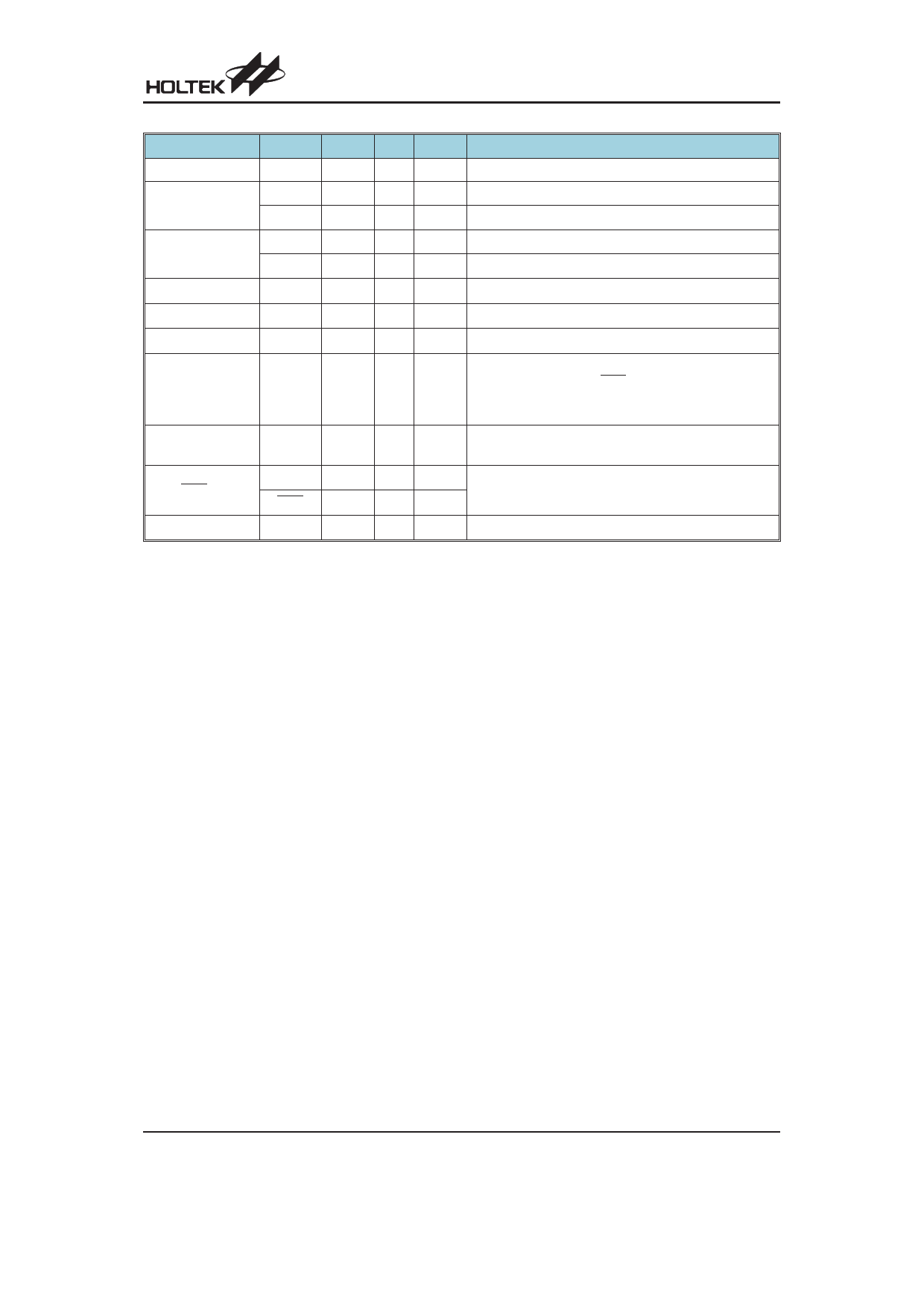
Pin Name
Function OPT I/T O/T
Description
PC1~PC5
PCn PCPU ST CMOS General purpose I/O. Register enabled pull-up.
PC6/CLK
PC6 PCPU ST CMOS General purpose I/O. Register enabled pull-up.
CLK
¾
ST
¾ VFD control interface
PC7/STROBE
PC7 PCPU ST CMOS General purpose I/O. Register enabled pull-up.
STROBE ¾
ST
¾ VFD control interface
VDD
VDD
¾ PWR ¾ Power supply
VSS
VSS
¾ PWR ¾ Ground
VFD23~VFD0
VCC
VFDn
VCC
¾
¾ HV High voltage grid/segment output for VFD panel
High voltage positive power supply for driving the VFD fil-
¾
PWR
¾
ament, F1O, BZO and BZO outputs. An external 10mF
capacitor is recommended to be connected to ground on
the PCB to reduce surge voltages.
VO
VO
¾
¾
PWR LDO regulator output (5V). It¢s be recommend that con-
necting an external capacitor on PCB layout.
BZO, BZO
BZO
BZO
¾
¾ HV
High voltage buzzer complement output signals
¾
¾ HV
F1O
F1O
¾
¾ HV High voltage filament output signal.
Note:
I/T: Input type; O/T: Output type
OPT: Optional by configuration option (CO) or register option
PWR: Power; CO: Configuration option
ST: Schmitt Trigger input; CMOS: CMOS output; AN: analog input
SCOM: Software controlled LCD COM
HXT: High frequency crystal oscillator
LXT: Low frequency crystal oscillator
HV : high voltage output
For VFD driver interface, the I/O function should only be configured as outputs.
Absolute Maximum Ratings
Supply Voltage ...........................VSS-0.3V to VSS+6.0V
Input Voltage..............................VSS-0.3V to VDD+0.3V
IOL Total ..............................................................100mA
Total Power Dissipation .....................................500mW
Storage Temperature ............................-50°C to 125°C
Operating Temperature...........................-40°C to 85°C
IOH Total............................................................-100mA
Note: These are stress ratings only. Stresses exceeding the range specified under ²Absolute Maximum Ratings² may
cause substantial damage to the device. Functional operation of this device at other conditions beyond those listed
in the specification is not implied and prolonged exposure to extreme conditions may affect device reliability.
Rev. 1.00
4
October 20, 2009
Share Link: 