DS1808 Просмотр технического описания (PDF) - Dallas Semiconductor -> Maxim Integrated
Номер в каталоге
Компоненты Описание
производитель
DS1808 Datasheet PDF : 17 Pages
| |||
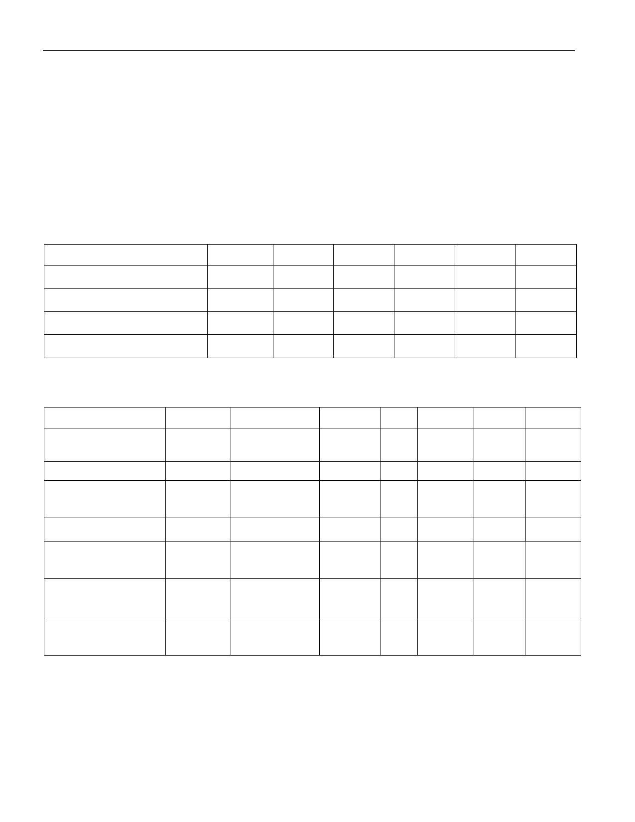
ABSOLUTE MAXIMUM RATINGS*
Voltage on All Pins (except /CE, SDA, SCL,
A0, A1, and A2) Relative to Ground
Voltage on Pins /CE, SDA, SCL, A0, A1, and A2
Operating Temperature
Storage Temperature
Soldering Temperature
VB - 0.3V to VCC + 0.3V
GND - 0.3V to VDD + 0.3V
-40°C to +85°C
-55°C to +125°C
See J-STD-020A specification
DS1808
*This is a stress rating only and functional operation of the device at these or any other conditions above
those indicated in the operation sections of this specification is not implied. Exposure to absolute
maximum rating conditions for extended periods of time may affect reliability.
RECOMMENDED DC OPERATING CONDITIONS
PARAMETER
SYMBOL MIN
TYP
Analog Supply Voltage
VCC
+4.5
Substrate Bias Voltage
VB
-13.2
Digital Supply Voltage
VDD
4.5
Resistor Inputs
L,H,W
VB
MAX
+13.2
0
5.5
VCC
(-40°C to +85°C)
UNITS NOTES
V
1, 3
V
3
V
3
V
DC ELECTRICAL CHARACTERISTICS
(-40°C to +85°C/VCC, VB=±5V to ±13.2V/VDD=4.5V to 5.5V)
PARAMETER
SYMBOL CONDITION MIN TYP MAX UNITS NOTES
Supply Current
ICC
Active
Input Leakage
ILI
Input Logic 1
VIH
-1
0.7VDD
2
mA
+1
mA
VDD +
0.3V
V
12, 13
2
Input Logic 0
VIL
GND-0.3
0.8
V
2
Power Up Time
(Port Active)
Standby Current
(VCC, VB)
Active Supply
Current (VB)
tPU
ISTBY
±8V
±12V
1
ms
15
mA
4
25
2.0
mA 12, 13
11 of 17
Share Link: 