CXD2931GA-9 Просмотр технического описания (PDF) - Sony Semiconductor
Номер в каталоге
Компоненты Описание
производитель
CXD2931GA-9 Datasheet PDF : 27 Pages
| |||
CXD2931R-9/GA-9
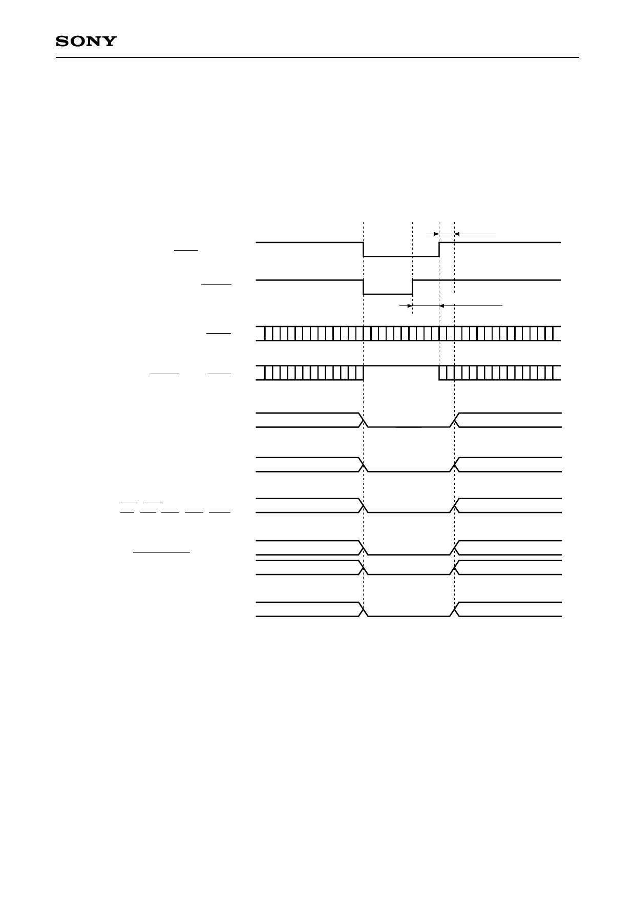
Battery Backup Mode
The battery backup mode is activated when the power for the GPS receiver is turned off and power-on reset
goes to low level. The timer clock continues to operate even when power-on reset goes low, but all other clock
are fixed high and the LSI is set to the low power consumption mode. At this time, the RAM data is held and
the registers are initialized.
Battery backup mode is canceled by setting power-on reset to high.
Power-on reset
EXRS
PWRST
Timer clocks
CCKI, CCKO
Other clocks
TCXO, XTCXO, CLKI, CLKO
Normal outputs
TXD0 to 2, OTCXO, HOLDA
Tri-state outputs
IODBK, RUN, CLKOUT
Tri-state outputs
ICS0, ICS1, IADR[18:1],
IRD, IWR, DRD, DWR, XCS0
Bidirectional
(Input)
SINT, IB[15:0], DCS0 to DCS5,
DADR[15:0], DB[7:0], PORT[22:0] (Outut)
Inputs
RXD0 to RXD2, IF0,
HOLD, NMI, PMI
10 clocks
100ms or more
Fixed low
Fixed low
Hi-Z
Fixed low
Hi-Z
Fixed low
– 11 –
Share Link: 