UDA1344TS Просмотр технического описания (PDF) - Philips Electronics
Номер в каталоге
Компоненты Описание
производитель
UDA1344TS Datasheet PDF : 28 Pages
| |||

Philips Semiconductors
Low-voltage low-power stereo audio
CODEC with DSP features
Product specification
UDA1344TS
L3 INTERFACE
The UDA1344TS has a microcontroller input mode. In the
microcontroller control mode, all the digital sound
processing features and the system controlling features
can be controlled by the microcontroller. The controllable
features are:
• System clock frequency
• Data input format
• Power control
• DC filtering
• De-emphasis
• Volume
• Flat/min./max. switch
• Bass boost
• Treble
• Mute.
The exchange of data and control information between the
microcontroller and the UDA1344TS is accomplished
through a serial hardware interface comprising the
following lines:
L3DATA: microcontroller interface data line
L3MODE: microcontroller interface mode line
L3CLOCK: microcontroller interface clock line.
Information transfer via the microcontroller bus is LSB first
and is organized in accordance with the so called
‘L3’ format, in which two different modes of operation can
be distinguished: address mode and data transfer mode.
The address mode is required to select a device
communicating via the L3 interface and to define the
destination registers for the data transfer mode. Data
transfer for the UDA1344TS can only be in one direction:
input to the UDA1344TS to program its sound processing
and other functional features.
Address mode
The address mode is used to select a device for
subsequent data transfer and to define the destination
registers. The address mode is characterized by L3MODE
being LOW and a burst of 8 pulses on L3CLOCK,
accompanied by 8 data bits.
The fundamental timing is shown in Fig.4.
Data bits 7 to 2 represent a 6-bit device address, with bit 7
being the MSB and bit 2 the LSB. The address of the
UDA1344TS is 000101 (bits 7 to 2).
Data bits 1 and 0 indicate the type of subsequent data
transfer as given in Table 13.
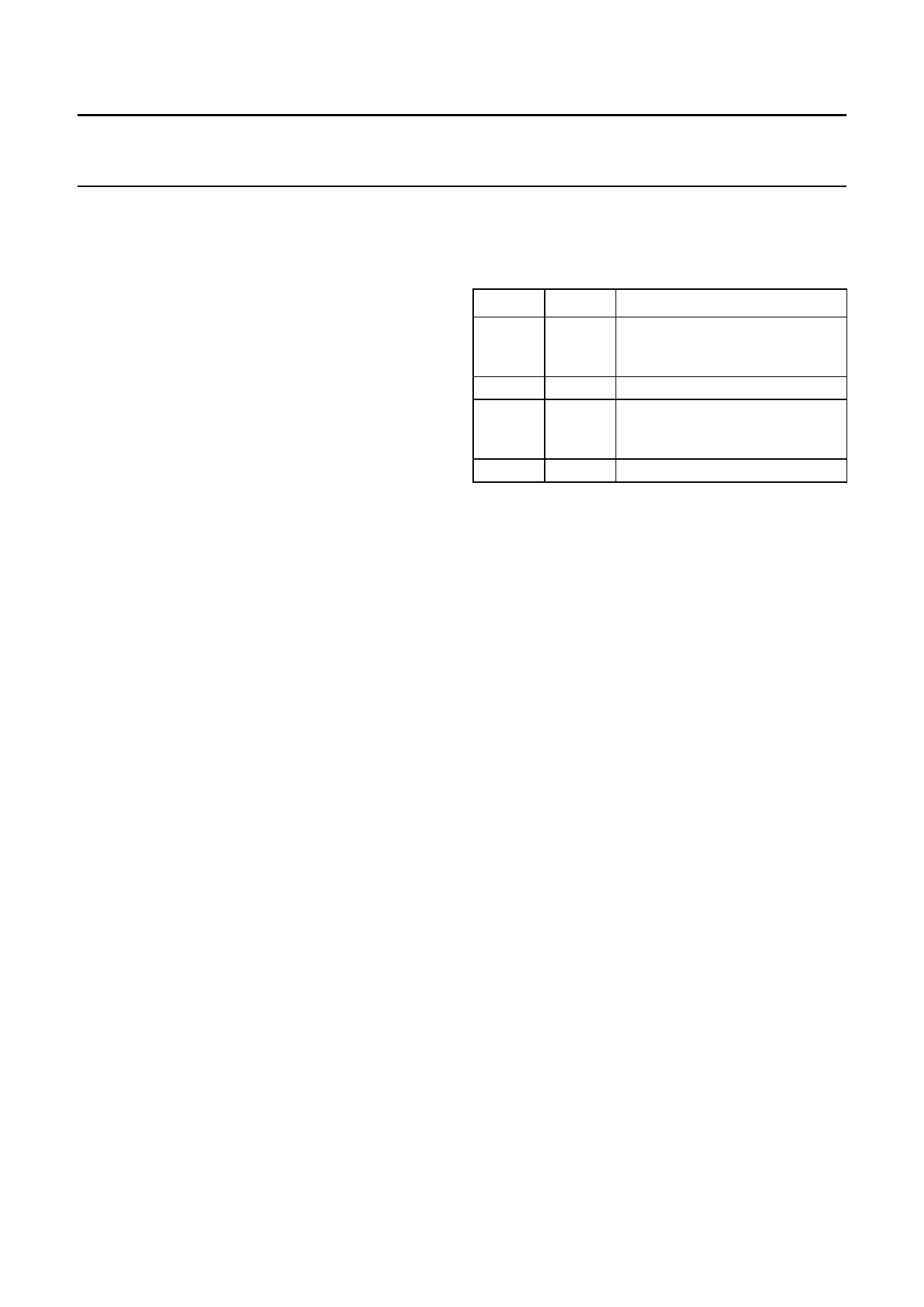
Table 13 Selection of data transfer
BIT 1
0
0
1
1
BIT 0
0
1
0
1
TRANSFER
data (volume, bass boost, treble,
de-emphasis, mute, mode and
power control)
not used
status (system clock frequency,
data input/output format and
DC filter)
not used
In the event that the UDA1344TS receives a different
address, it will deselect its microcontroller interface logic.
Data transfer mode
The selection preformed in the address mode remains
active during subsequent data transfers, until the
UDA1344TS receives a new address command.
The fundamental timing of data transfers is essentially the
same as in the address mode and is shown in Fig.5.
The maximum input clock and data rate is 64fs.
All transfers are byte wise, i.e. they are based on groups
of 8 bits. Data will be stored in the UDA1344TS after the
eighth bit of a byte has been received.
A multibyte data transfer is illustrated in Fig.6.
Programming the sound processing and other
features
The sound processing and other feature values are stored
in independent registers.
The first selection of the registers is achieved by the choice
of data type that is transferred. This is performed in the
address mode by bit 1 and bit 0 (see Table 13).
The second selection is performed by the 2 MSBs of the
data byte (bit 7 and bit 6).
The other bits in the data byte (bits 5 to 0) is the value that
is placed in the selected registers.
2001 Jun 29
11