AM79C02 Просмотр технического описания (PDF) - Advanced Micro Devices
Номер в каталоге
Компоненты Описание
производитель
AM79C02 Datasheet PDF : 48 Pages
| |||
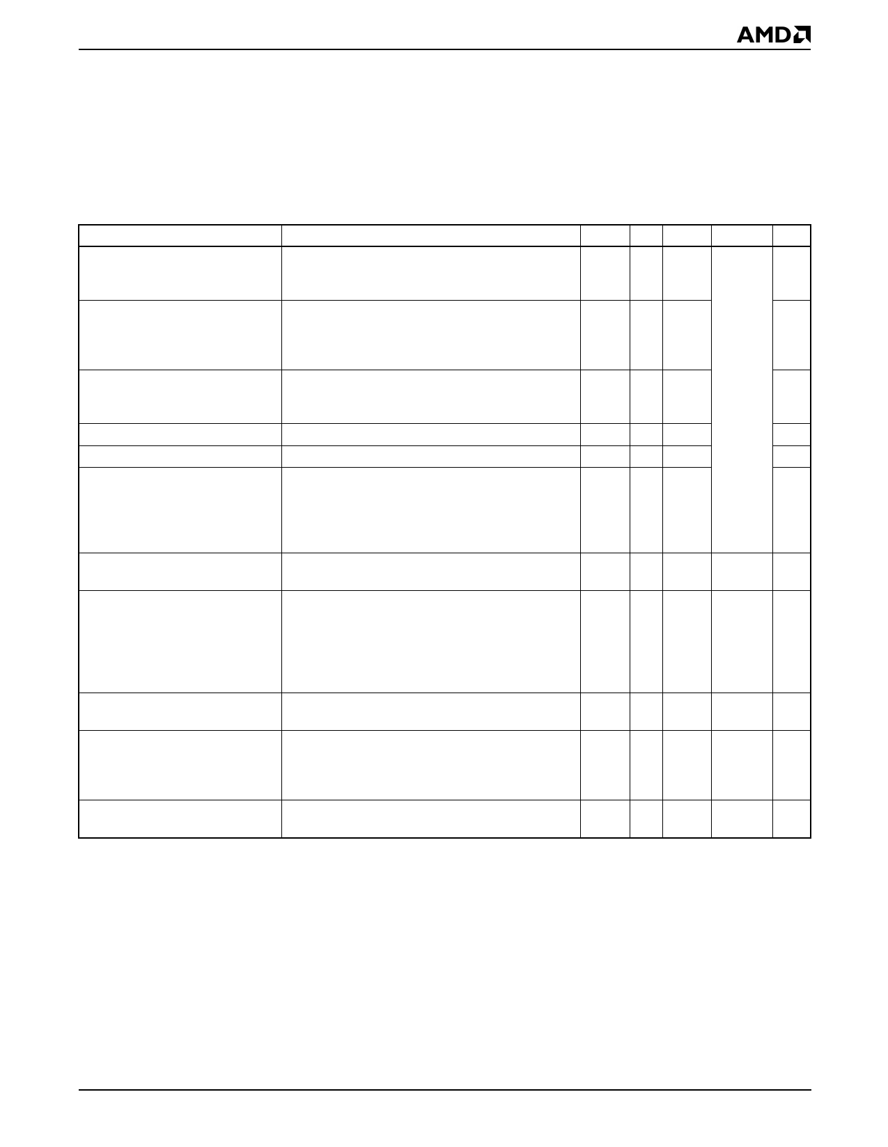
Transmission Characteristics
The gain of the receive path is defined to be 0 dB when a 0 dBm0, 1014 Hz PCM sine wave input results in a nominal
1.55 Vrms for µ-law or 1.56 Vrms for A-law analog output. The gain of the transmit path is 0 dB when a 1.55 Vrms
for µ-law or 1.56 Vrms for A-law, 1014 Hz sine wave analog input results in a level of 0 dBm0 at the digital output.
When relative levels (dBm0) are used in any of the following transmission specifications, the specification holds for any
setting of the AX + GX gain from 0 to 12 dB and the AR + GR loss from 0 to 12 dB. Performance specification for
settings of the AX + GX gain from 12 to 18 dB and the AR + GR loss from 12 to 18 dB is determined as the device
is characterized.
Description
Test Conditions
Min Typ Max Unit Note
Gain accuracy
D to A or A to D
0 dBm0, 1014 Hz
0 dB < |path gain| < 6 dB
25°C to 85°C
0°C
–40°C
–0.20
–0.25
–0.35
+0.20
+0.25
+0.35
Gain accuracy
D to A or A to D
0 dBm0, 1014 Hz
70°C to 85°C –0.20
+0.20
—
6 dB < |path gain| < 12 dB
25°C –0.25
+0.25
1
0°C –0.30
+0.30
1
–40°C –0.35
+0.35
—
Gain accuracy
analog to analog
or digital to digital
25°C to 85°C
0°C
–40°C
–0.20
–0.25
–0.35
+0.20
+0.25 dB
+0.35
Attenuation distortion
300 Hz to 3400 Hz –0.125
+0.125
2
Single frequency distortion, A to D
–46
3
Single frequency distortion, D to A –6 dB < (GR + AR) < 0 dB
–12 dB < (GR + AR) < –6 dB
–12 dB < (GR + AR) < –6 dB
–12 dB < (GR + AR) < –6 dB
–12 dB < (GR + AR) < –6 dB
–40°C to 85°C
70°C to 85°C
25°C
0°C
–40°C
–46
3
–46
3
–45
3, 4
–43
3, 4
–40
3, 4
Intermodulation distortion
–42
–56
dBr
5
Analog out digital looped back
Idle channel noise
digital input = 0
Digital out analog VIN = 0
weighted
unweighted
A-law
µ-law
A-law
µ-law
–68 dBm0p
–55 dBm0p
–78 dBm0p
12 dBrnc0
6
–68 dBm0p
19 dBrnc0
Crosstalk
same channel
TX to RX
RX to TX
0 dBm0
300 Hz to 3400 Hz
–75
–75
Crosstalk
between channels
TX to TX
TX to RX
RX to TX
RX to RX
0 dBm0
–76
300 Hz to 3400 Hz
–78
–76
–78
Group delay
PCLK ≥ 1.53 MHz
PCLK ≤ 1.03 MHz
B, X, R, and Z filters disabled
630
695
µs
7
Notes:
1. AMD guarantees less than 0.1% of units fall into the last 0.05 dB of these specification numbers.
2. See Figure 1.
3. With f swept between 0 to 300 Hz and 3400 to 12 kHz, any generated output signals other than f are less than –28 dBm0.
This specification is valid for either transmission path.
4. AMD guarantees < 0.2% of units are above –46 dB. This relaxed specification applies to only the third harmonic.
5. Intermodulation distortion specification for two signals of same level in the range of –4 dBm0 to –21 dBm0 does not produce
2 • (f1 – f2) component above specified level. 50 Hz IMD specified with 50 Hz signal at –23 dBm0 and signal between 300 Hz
to 3400 Hz at –9 dBm0.
6. No single frequency component in the range above 3800 Hz may exceed a level of –55 dBm0.
7. The Group Delay specification is defined as the sum of the minimum values of the group delays for the transmit and the
receive paths when the transmit and receive time slots are identical and the B, X, R, and Z filters are disabled. For PCLK
frequencies between 1.03 MHz and 1.53 MHz, the group delay may vary from one cycle to the next. See Figure 2.
SLAC Products
11
Share Link: 