ADSP-2196MKCA-160X Просмотр технического описания (PDF) - Analog Devices
Номер в каталоге
Компоненты Описание
производитель
ADSP-2196MKCA-160X Datasheet PDF : 68 Pages
| |||
35(/,0,1$5< 7(&+1,&$/ '$7$
September 2001 For current information contact Analog Devices at 800/262-5643
ADSP-2196
Two mode bits in the Host Port configuration register
HPCR [7:6] define the functionality of the HACK line.
HPCR6 is initialized at reset based on the values driven on
HACK and HACK_P pins (shown in Table 5); HPCR7 is
always cleared (0) at reset. HPCR [7:6] can be modified
after reset by a write access to the host port
configuration register.
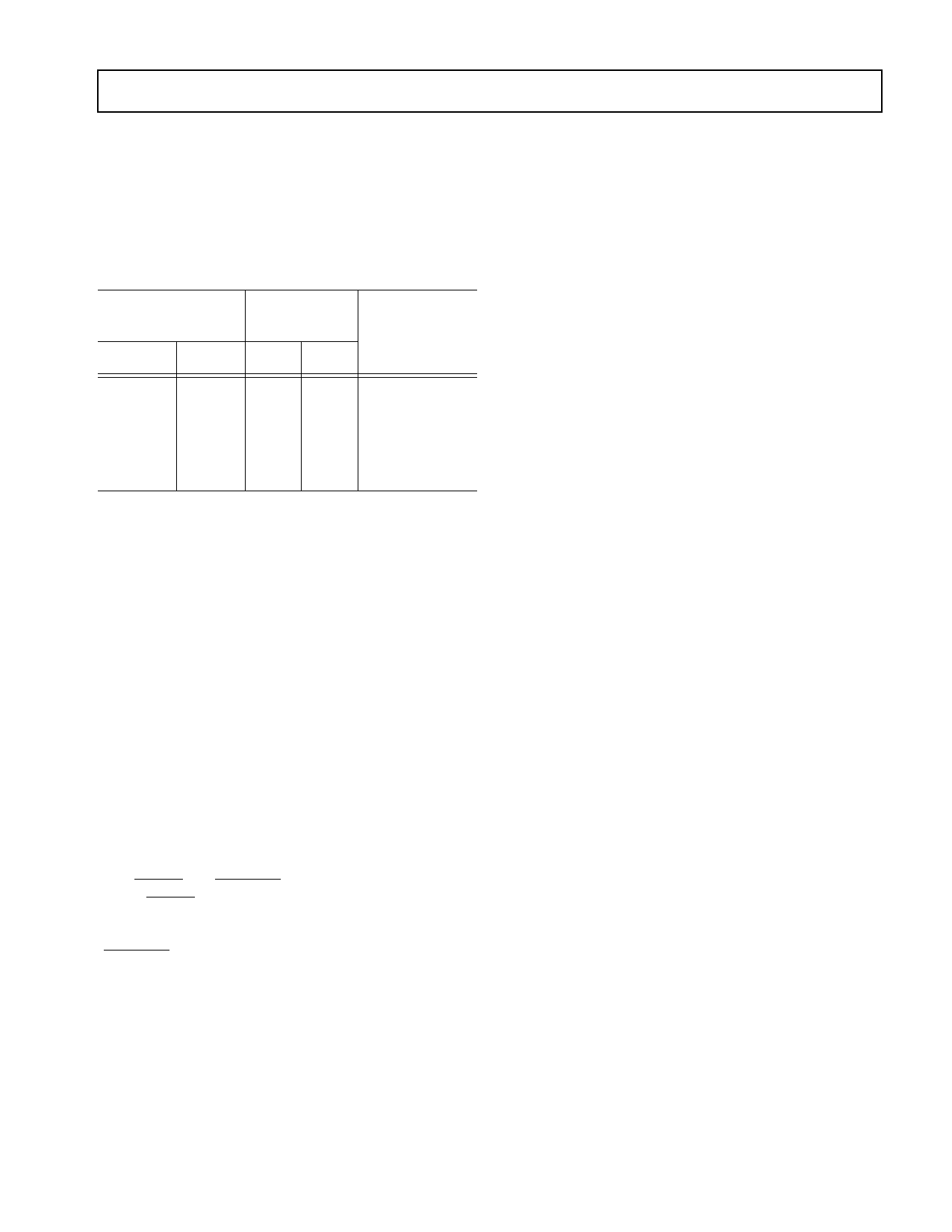
Table 5. Host Port Acknowledge Mode Selection
Values Driven At
Reset
HACK_P HACK
0
0
0
1
1
0
1
1
HPCR [7:6]
Initial Values
Bit 7
0
0
0
0
Bit 6
1
0
0
1
Acknowledge
Mode
Ready Mode
ACK Mode
ACK Mode
Ready Mode
The functional modes selected by HPCR [7:6] are as follows
(assuming active high signal):
• ACK Mode—Acknowledge is active on strobes; HACK
goes high from the leading edge of the strobe to indicate
when the access can complete. After the Host samples the
HACK active, it can complete the access by removing the
strobe.The host port then removes the HACK.
• Ready Mode—Ready active on strobes, goes low to insert
wait state during the access.If the host port can not
complete the access, it de-asserts the HACK/READY
line. In this case, the Host has to extend the access by
keeping the strobe asserted. When the Host samples the
HACK asserted, it can then proceed and complete the
access by de-asserting the strobe.
While in Address Cycle Control (ACC) mode and the ACK
or Ready acknowledge modes, the HACK is returned active
for any address cycle.
Host Port Chip Selects
There are two chip-select signals associated with the Host
Port: HCMS and HCIOMS. The Host Chip Memory
Select (HCMS) lets the Host select the DSP and directly
access the DSP’s internal/external memory space or boot
memory space. The Host Chip I/O Memory Select
(HCIOMS) lets the Host select the DSP and directly access
the DSP’s internal I/O memory space.
Before starting a direct access, the Host configures Host
port interface registers, specifying the width of external data
bus (8- or 16-bit) and the target address page (in the IJPG
register). The DSP generates the needed memory select
signals during the access, based on the target address. The
Host port interface combines the data from one, two, or
three consecutive Host accesses (up to one 24-bit value) into
a single DMA bus access to prefetch Host direct reads or to
post direct writes. During assembly of larger words, the Host
port interface asserts ACK for each byte access that does
not start a read or complete a write. Otherwise, the Host
port interface asserts ACK when it has completed the
memory access successfully.
DSP Serial Ports (SPORTs)
The ADSP-2196 incorporates three complete synchronous
serial ports (SPORT0, SPORT1, and SPORT2) for serial
and multiprocessor communications. The SPORTs
support the following features:
• Bidirectional operation—each SPORT has independent
transmit and receive pins.
• Buffered (8-deep) transmit and receive ports—each port
has a data register for transferring data words to and from
other DSP components and shift registers for shifting data
in and out of the data registers.
• Clocking—each transmit and receive port can either use
an external serial clock (≤75 MHz) or generate its own,
in frequencies ranging from 1144 Hz to 75 MHz.
• Word length—each SPORT supports serial data words
from 3 to 16 bits in length transferred in Big Endian
(MSB) or Little Endian (LSB) format.
• Framing—each transmit and receive port can run with or
without frame sync signals for each data word. Frame sync
signals can be generated internally or externally, active
high or low, and with either of two pulsewidths and early
or late frame sync.
• Companding in hardware—each SPORT can perform
A-law or µ-law companding according to ITU recommen-
dation G.711. Companding can be selected on the
transmit and/or receive channel of the SPORT without
additional latencies.
• DMA operations with single-cycle overhead—each
SPORT can automatically receive and transmit multiple
buffers of memory data, one data word each DSP cycle.
Either the DSP’s core or a Host processor can link or chain
sequences of DMA transfers between a SPORT and
memory. The chained DMA can be dynamically allocated
and updated through the DMA descriptors (DMA
transfer parameters) that set up the chain.
• Interrupts—each transmit and receive port generates an
interrupt upon completing the transfer of a data word or
after transferring an entire data buffer or buffers through
DMA.
• Multichannel capability—each SPORT supports the
H.100 standard.
REV. PrA
This information applies to a product under development. Its characteristics and specifications are subject to change with-
11
out notice. Analog Devices assumes no obligation regarding future manufacturing unless otherwise agreed to in writing.
Share Link: 