ADCMP563BCPZ-RL7(RevD) Просмотр технического описания (PDF) - Analog Devices
Номер в каталоге
Компоненты Описание
производитель
ADCMP563BCPZ-RL7 Datasheet PDF : 15 Pages
| |||
Data Sheet
Dual, High Speed ECL Comparators
ADCMP563/ADCMP564
FEATURES
Differential ECL-compatible outputs
700 ps propagation delay input to output
75 ps propagation delay dispersion
Input common-mode range: –2.0 V to +3.0 V
Robust input protection
Differential latch control
Internal latch pull-up resistors
Power supply rejection greater than 85 dB
700 ps minimum pulse width
1.5 GHz equivalent input rise time bandwidth
Typical output rise/fall time of 500 ps
ESD protection > 4kV HBM, >200V MM
Programmable hysteresis
APPLICATIONS
Automatic test equipment
High speed instrumentation
Scope and logic analyzer front ends
Window comparators
High speed line receivers
Threshold detection
Peak detection
High speed triggers
Patient diagnostics
Hand-held test instruments
Zero crossing detectors
Line receivers and signal restoration
Clock drivers
GENERAL DESCRIPTION
The ADCMP563/ADCMP564 are high speed comparators
fabricated on Analog Devices’ proprietary XFCB process. The
devices feature a 700 ps propagation delay with less than 75 ps
overdrive dispersion. Dispersion, a measure of the difference in
propagation delay under differing overdrive conditions, is a partic-
ularly important characteristic of high speed comparators. A separate
programmable hysteresis pin is available on the ADCMP564.
A differential input stage permits consistent propagation delay
with a wide variety of signals in the common-mode range from
−2.0 V to +3.0 V. Outputs are complementary digital signals that
are fully compatible with ECL 10 K and 10 KH logic families.
The outputs provide sufficient drive current to directly drive
transmission lines terminated in 50 Ω to −2 V. A latch input,
which is included, permits tracking, track-and-hold, or sample-
and-hold modes of operation. The latch input pins contain internal
pull-ups that set the latch in tracking mode when left open.
The ADCMP563/ADCMP564 are specified over the industrial
temperature range (−40°C to +85°C).
Rev. D
Document Feedback
Information furnished by Analog Devices is believed to be accurate and reliable. However, no
responsibility is assumed by Analog Devices for its use, nor for any infringements of patents or other
rights of third parties that may result from its use. Specifications subject to change without notice. No
license is granted by implication or otherwise under any patent or patent rights of Analog Devices.
Trademarks and registered trademarks are the property of their respective owners.
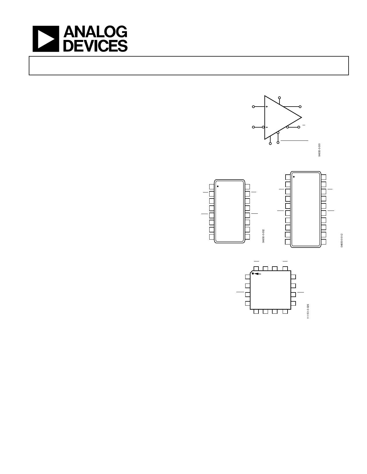
FUNCTIONAL BLOCK DIAGRAMS
HYS*
NONINVERTING
INPUT
INVERTING
INPUT
ADCMP563/
ADCMP564
Q OUTPUT
Q OUTPUT
LATCH ENABLE
INPUT
LATCH ENABLE
INPUT
*ADCMP564 ONLY
Figure 1.
QA 1
16 QB
QA 2
15 QB
GND 3
LEA 4
LEA 5
VEE 6
–INA 7
ADCMP563
BRQ
TOP VIEW
(Not to Scale)
14 GND
13 LEB
12 LEB
11 VCC
10 –INB
+INA 8
9 +INB
Figure 2. ADCMP563 16-Lead QSOP
GND 1
20 GND
QA 2
19 QB
QA 3
GND 4
LEA 5
LEA 6
18 QB
ADCMP564 17 GND
BRQ
TOP VIEW 16 LEB
(Not to Scale) 15 LEB
VEE 7
–INA 8
14 VCC
13 –INB
+INA 9
12 +INB
HYSA 10
11 HYSB
Figure 3. ADCMP564 20-Lead QSOP
–INA 1
+INA 2
+INB 3
–INB 4
ADCMP563
BCP
TOP VIEW
(Not to Scale)
12 QA
11 QA
10 QB
9 QB
NOTES
1. THE EXPOSED PAD SHOULD BE EITHER CONNECTED TO VEE OR LEFT FLOATING.
Figure 4. ADCMP563 16-Lead LFCSP
One Technology Way, P.O. Box 9106, Norwood, MA 02062-9106, U.S.A.
Tel: 781.329.4700 ©2007–2016 Analog Devices, Inc. All rights reserved.
Technical Support
www.analog.com
Share Link: 