EVAL-AD5750EBZ(RevF) Просмотр технического описания (PDF) - Analog Devices
Номер в каталоге
Компоненты Описание
производитель
EVAL-AD5750EBZ
(Rev.:RevF)
(Rev.:RevF)
Analog Devices

EVAL-AD5750EBZ Datasheet PDF : 36 Pages
| |||
AD5750/AD5750-1/AD5750-2
Data Sheet
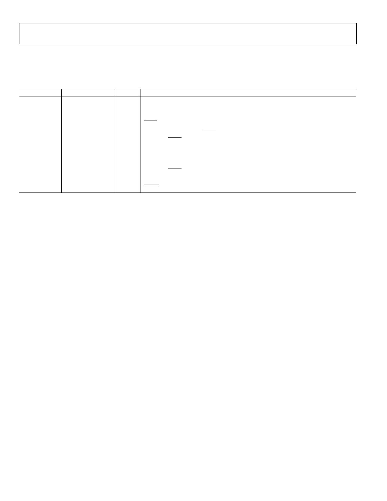
TIMING CHARACTERISTICS
AVDD/AVSS = ±12 V (± 10%) to ±24 V (± 10%), DVCC = 2.7 V to 5.5 V, GND = 0 V. VOUT: RLOAD = 2 kΩ, CL = 200 pF, IOUT: RLOAD =
300 Ω. All specifications TMIN to TMAX, unless otherwise noted.
Table 3.
Parameter1, 2
t1
t2
t3
t4
t5
t6
t7
t8
t9, t10
t11
t12
t13
Limit at TMIN, TMAX
20
8
8
5
10
5
5
5
1.5
5
40
10
Unit
ns min
ns min
ns min
ns min
ns min
ns min
ns min
ns min
µs max
ns min
ns max
ns min
Description
SCLK cycle time
SCLK high time
SCLK low time
SYNC falling edge to SCLK falling edge setup time
16th SCLK falling edge to SYNC rising edge (on 24th SCLK falling edge if using PEC)
Minimum SYNC high time (write mode)
Data setup time
Data hold time
CLEAR pulse low/high activation time
Minimum SYNC high time (read mode)
SCLK rising edge to SDO valid (SDO CL = 15 pF)
RESET pulse low time
1 Guaranteed by characterization, but not production tested.
2 All input signals are specified with tR = tF = 5 ns (10% to 90% of DVCC) and timed from a voltage level of 1.2 V.
Rev. F | Page 8 of 36
Share Link: