AD5533BBCZ-1 Просмотр технического описания (PDF) - Analog Devices
Номер в каталоге
Компоненты Описание
производитель
AD5533BBCZ-1 Datasheet PDF : 16 Pages
| |||
AD5533B
FUNCTIONAL DESCRIPTION
The AD5533B can be thought of as consisting of an ADC and
32 DACs in a single package. The input voltage VIN is sampled
and converted into a digital word. The digital result is loaded into
one of the DAC registers and is converted (with gain and offset)
into an analog output voltage (VOUT0–VOUT31). Since the chan-
nel output voltage is effectively the output of a DAC there is no
droop associated with it. As long as power to the device is main-
tained, the output voltage will remain constant until this channel
is addressed again.
To update a single channel’s output voltage, the required new
voltage level is set up on the common input pin, VIN. The desired
channel is then addressed via the parallel port or the serial port.
When the channel address has been loaded, provided TRACK is
high, the circuit begins to acquire the correct code to load to the
DAC so that the DAC output matches the voltage on VIN. The
BUSY pin goes low and remains so until the acquisition is com-
plete. The noninverting input to the output buffer is tied to VIN
during the acquisition period to avoid spurious outputs while the
DAC acquires the correct code. The acquisition is completed in
16 µs max. The BUSY pin goes high and the updated DAC output
assumes control of the output voltage. The output voltage of the
DAC is connected to the noninverting input of the output buffer.
Since the internal DACs are offset by 70 mV (max) from GND,
the minimum VIN in ISHA mode is 70 mV. The maximum VIN is
2.96 V due to the upper dead band of 40 mV (max).
On power-on, all the DACs, including the offset channel, are loaded
with zeros. Each of the 33 DACs is offset internally by 50 mV (typ)
from GND so the outputs VOUT0 to VOUT31 are 50 mV (typ) on
power-on if the OFFS_IN pin is driven directly by the on-board
offset channel (OFFS_OUT), i.e., if OFFS_IN = OFFS_OUT =
50 mV = > VOUT = (Gain ϫ VDAC) – (Gain – 1) ϫ VOFFS_IN = 50 mV.
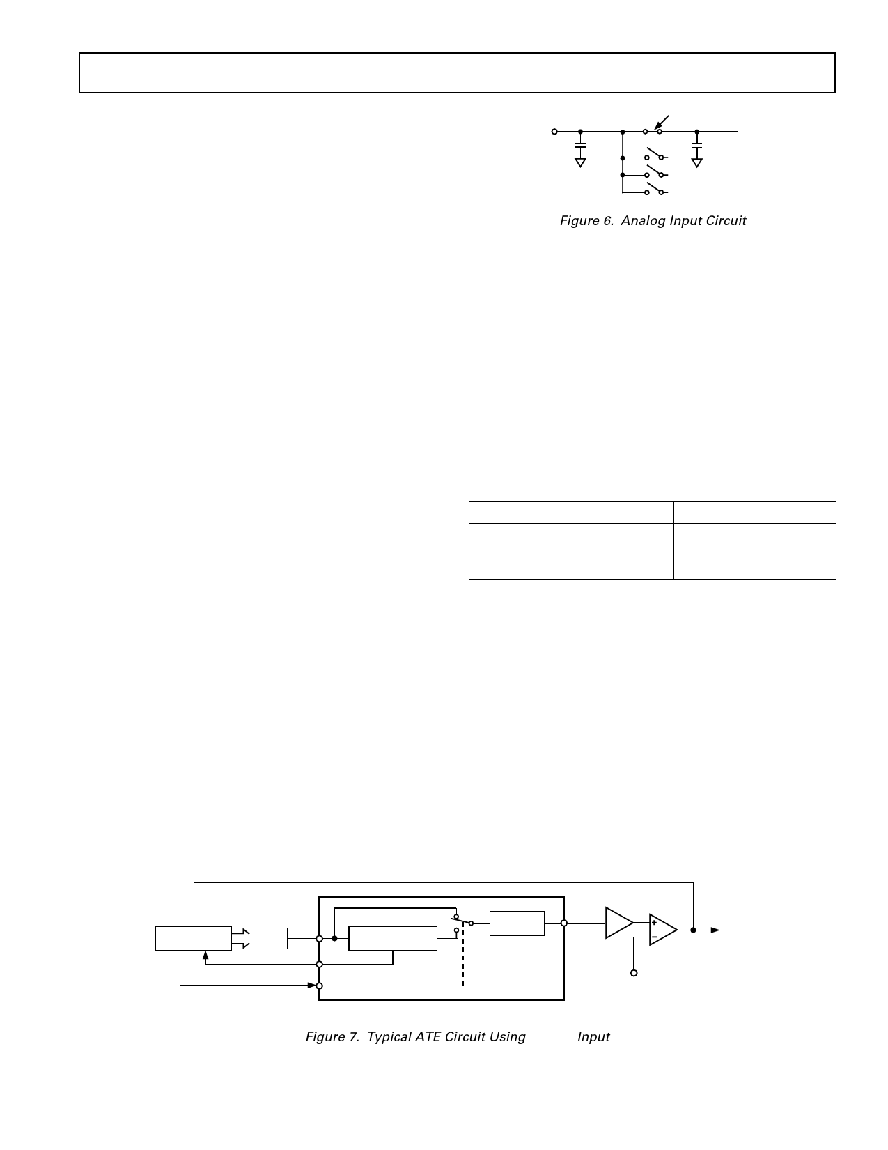
Analog Input
The equivalent analog input circuit is shown in Figure 6. The
capacitor C1 is typically 20 pF and can be attributed to pin capaci-
tance and 32 off-channels. When a channel is selected, an extra
7.5 pF (typ) is switched in. This capacitor C2 is charged to the
previously acquired voltage on that particular channel so it must
charge/discharge to the new level. It is essential that the external
source can charge/discharge this additional capacitance within
1 µs–2 µs of channel selection so that VIN can be acquired accu-
rately. For this reason, a low impedance source is recommended.
VIN
C1
20pF
ADDRESSED CHANNEL
C2
7.5pF
Figure 6. Analog Input Circuit
Large source impedances will significantly affect the performance
of the ADC. This may necessitate the use of an input buffer
amplifier.
Output Buffer Stage—Gain and Offset
The function of the output buffer stage is to translate the
50 mV–3 V typical output of the DAC to a wider range. This
is done by gaining up the DAC output by 3.52 and offsetting
the voltage by the voltage on OFFS_IN pin.
VOUT = 3.52 ×VDAC − 2.52 ×VOFFS_IN
VDAC is the output of the DAC.
VOFFS_IN is the voltage at the OFFS_IN pin.
Table I shows how the output range on VOUT relates to the
offset voltage supplied by the user.
Table I. Sample Output Voltage Ranges
VOFFS_IN (V)
0
1
2.130
VDAC (V)
0.05 to 3
0.05 to 3
0.05 to 3
VOUT (V)
0.176 to 10.56
–2.34 to +8.04
–5.192 to +5.192
VOUT is limited only by the headroom of the output amplifiers.
VOUT must be within maximum ratings.
Offset Voltage Channel
The offset voltage can be externally supplied by the user at
OFFS_IN or it can be supplied by an additional offset voltage
channel on the device itself. The required offset voltage is set up
on VIN and acquired by the offset DAC. This offset channel’s DAC
output is directly connected to OFFS_OUT. By connecting
OFFS_OUT to OFFS_IN, this offset voltage can be used as the
offset voltage for the 32 output amplifiers. It is important to
choose the offset so that VOUT is within maximum ratings.
CCOONNTTRROOLLLLEERR
VIN
DAC
BUSY
TRACK
AACCQQUUISISITITIOIONN
CCIRIRCCUUITIT
OUTPUT
STAGE
AD5533B
ONLY ONE CHANNEL SHOWN FOR SIMPLICITY
PIN
DRIVER
VOUT1
THRESHOLD
VOLTAGE
Figure 7. Typical ATE Circuit Using TRACK Input
DEVICE
UNDER
TEST
REV. A
–11–
Share Link: 