AD5533BBCZ-1 Просмотр технического описания (PDF) - Analog Devices
Номер в каталоге
Компоненты Описание
производитель
AD5533BBCZ-1 Datasheet PDF : 16 Pages
| |||
AD5533B
ISHA
ISHA
ISHA
ACTIVE
LOAD
PARAMETRIC
MEASUREMENT SYSTEM BUS
UNIT
STORED
DATA
AND INHIBIT
PATTERN
PERIOD
GENERATION
AND
DELAY
TIMING
DRIVER
ISHA
FORMATTER
ISHA
COMPARE
REGISTER
ISHAs
SYSTEM BUS
COMPARATOR
ISHA
ISHA
DUT
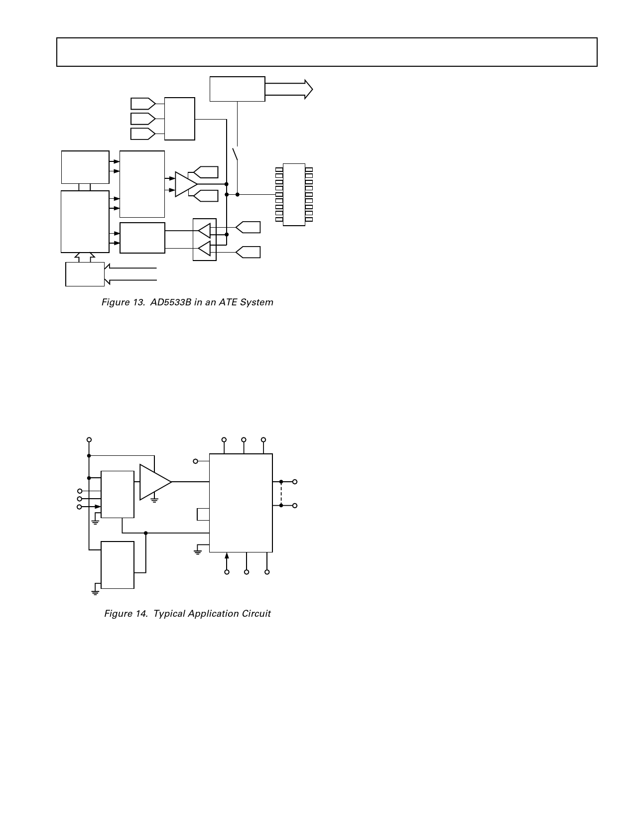
Figure 13. AD5533B in an ATE System
Typical Application Circuit
The AD5533B can be used to set up voltage levels on 32 channels as
shown in the circuit below. An AD780 provides the 3 V reference
for the AD5533B, and for the AD5541 16-bit DAC. A simple 3-wire
serial interface is used to write to the AD5541. Because the AD5541
has an output resistance of 6.25 kΩ (typ), the time taken to charge/
discharge the capacitance at the VIN pin is significant. Thus an
AD820 is used to buffer the DAC output. Note that it is important
to minimize noise on VIN and REFIN when laying out this circuit.
AVCC
AVCC DVCC VSS
CS
DIN
SCLK
VDD
AD5541* AD820
REF
VIN
AD5533B*
OFFS_IN
OFFS_OUT
REFIN
VOUT 0–31
AD780*
VOUT
SCLK DIN SYNC
*ADDITIONAL PINS OMITTED FOR CLARITY
Figure 14. Typical Application Circuit
POWER SUPPLY DECOUPLING
In any circuit where accuracy is important, careful consideration
of the power supply and ground return layout helps to ensure
the rated performance. The printed circuit board on which the
AD5533B is mounted should be designed so that the analog
and digital sections are separated and confined to certain areas
of the board. If the AD5533B is in a system where multiple
devices require an AGND-to-DGND connection, the connection
should be made at one point only. The star ground point should
be established as close as possible to the device. For supplies with
multiple pins (VSS, VDD, AVCC) it is recommended to tie those
pins together. The AD5533B should have ample supply bypass-
ing of 10 µF in parallel with 0.1 µF on each supply located as
close to the package as possible, ideally right up against the device.
The 10 µF capacitors are the tantalum bead type. The 0.1 µF
capacitor should have low effective series resistance (ESR) and
effective series inductance (ESI), like the common ceramic types
that provide a low impedance path to ground at high frequencies,
to handle transient currents due to internal logic switching.
The power supply lines of the AD5533B should use as large a trace
as possible to provide low impedance paths and reduce the effects
of glitches on the power supply line. Fast switching signals such
as clocks should be shielded with digital ground to avoid radiating
noise to other parts of the board, and should never be run near
the reference inputs. A ground line routed between the DIN and
SCLK lines will help reduce crosstalk between them (not required
on a multilayer board as there will be a separate ground plane,
but separating the lines will help). It is essential to minimize
noise on VIN and REFIN lines.
Note it is essential to minimize noise on VIN and REFIN lines.
Particularly for optimum ISHA performance, the VIN line must
be kept noise-free. Depending on the noise performance of the
board, a noise filtering capacitor may be required on the VIN line.
If this capacitor is necessary, then for optimum throughput it may
be necessary to buffer the source that is driving VIN. Avoid cross-
over of digital and analog signals. Traces on opposite sides of the
board should run at right angles to each other. This reduces the
effects of feedthrough through the board. A microstrip technique is
by far the best, but not always possible with a double-sided board.
In this technique, the component side of the board is dedicated
to ground plane while signal traces are placed on the solder side.
As is the case for all thin packages, care must be taken to avoid
flexing the CSPBGA package and to avoid a point load on the
surface of this package during the assembly process.
REV. A
–15–
Share Link: 