K20P64M72SF1 Просмотр технического описания (PDF) - Freescale Semiconductor
Номер в каталоге
Компоненты Описание
производитель
K20P64M72SF1
Freescale Semiconductor

K20P64M72SF1 Datasheet PDF : 67 Pages
| |||
General
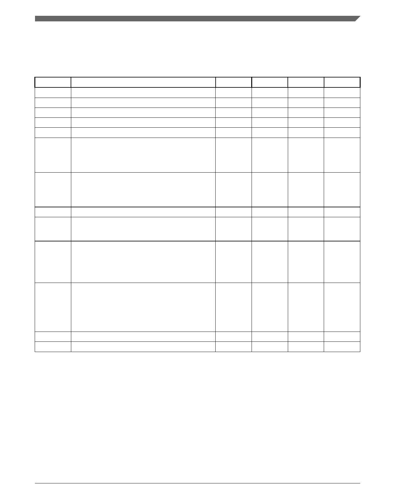
5.2.1 Voltage and current operating requirements
Table 1. Voltage and current operating requirements
Symbol Description
VDD
Supply voltage
VDDA Analog supply voltage
VDD – VDDA VDD-to-VDDA differential voltage
VSS – VSSA VSS-to-VSSA differential voltage
VBAT RTC battery supply voltage
VIH
Input high voltage
• 2.7 V ≤ VDD ≤ 3.6 V
• 1.7 V ≤ VDD ≤ 2.7 V
Min.
1.71
1.71
–0.1
–0.1
1.71
0.7 × VDD
0.75 × VDD
VIL
Input low voltage
• 2.7 V ≤ VDD ≤ 3.6 V
—
• 1.7 V ≤ VDD ≤ 2.7 V
—
VHYS
IICDIO
Input hysteresis
Digital pin negative DC injection current — single pin
• VIN < VSS-0.3V
0.06 × VDD
-5
IICAIO
Analog2, EXTAL, and XTAL pin DC injection current —
single pin
• VIN < VSS-0.3V (Negative current injection)
-5
• VIN > VDD+0.3V (Positive current injection)
—
IICcont
Contiguous pin DC injection current —regional limit,
includes sum of negative injection currents or sum of
positive injection currents of 16 contiguous pins
• Negative current injection
-25
• Positive current injection
—
Max.
3.6
3.6
0.1
0.1
3.6
—
—
0.35 × VDD
0.3 × VDD
—
—
—
+5
—
+25
Unit
V
V
V
V
V
V
V
V
V
V
mA
mA
mA
VRAM VDD voltage required to retain RAM
1.2
—
V
VRFVBAT VBAT voltage required to retain the VBAT register file
VPOR_VBAT
—
V
Notes
1
3
1. All 5 V tolerant digital I/O pins are internally clamped to VSS through a ESD protection diode. There is no diode connection
to VDD. If VIN greater than VDIO_MIN (=VSS-0.3V) is observed, then there is no need to provide current limiting resistors at
the pads. If this limit cannot be observed then a current limiting resistor is required. The negative DC injection current
limiting resistor is calculated as R=(VDIO_MIN-VIN)/|IIC|.
2. Analog pins are defined as pins that do not have an associated general purpose I/O port function.
3. All analog pins are internally clamped to VSS and VDD through ESD protection diodes. If VIN is greater than VAIO_MIN
(=VSS-0.3V) and VIN is less than VAIO_MAX(=VDD+0.3V) is observed, then there is no need to provide current limiting
resistors at the pads. If these limits cannot be observed then a current limiting resistor is required. The negative DC
injection current limiting resistor is calculated as R=(VAIO_MIN-VIN)/|IIC|. The positive injection current limiting resistor is
calculated as R=(VIN-VAIO_MAX)/|IIC|. Select the larger of these two calculated resistances.
K20 Sub-Family Data Sheet, Rev. 3, 11/2012.
Freescale Semiconductor, Inc.
11
Share Link: