MAX3349EA Просмотр технического описания (PDF) - Maxim Integrated
Номер в каталоге
Компоненты Описание
производитель
MAX3349EA Datasheet PDF : 17 Pages
| |||
USB 2.0 Full-Speed Transceiver with UART
Multiplexing Mode
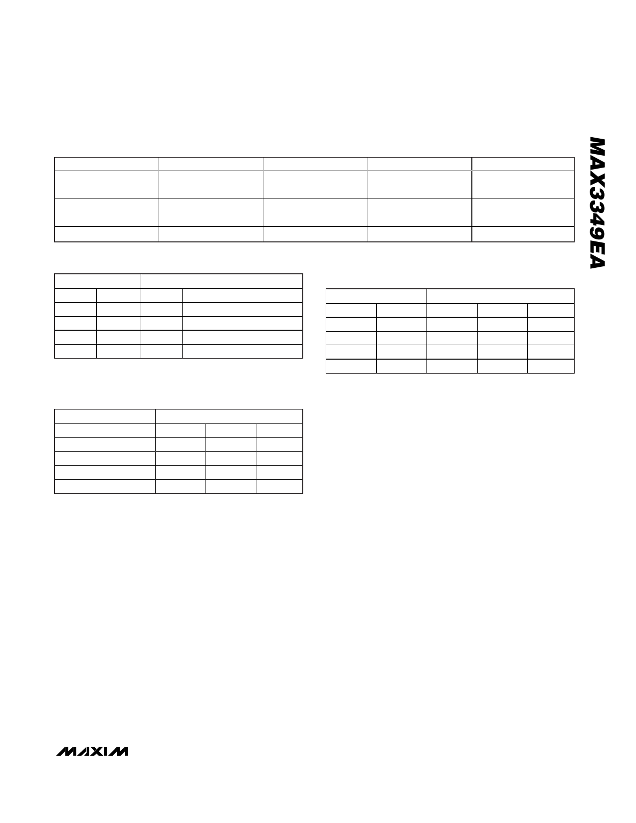
Table 1. Power-Supply Configuration
VBUS(V)
+4.0 to +5.5
+4.0 to +5.5
GND or Unconnected
VTRM(V)
+3.0 to +3.6 Output
+3.0 to +3.6 Output
High Impedance
VL(V)
+1.4 to +2.75
GND or Unconnected
+1.4 to +2.75
VUART(V)
GND, Unconnected, or
+2.7V to +3.3V
GND, Unconnected, or
+2.7V to +3.3V
+2.7V to +3.3V
CONFIGURATION
USB Mode
Disable Mode
UART Mode
Table 2. USB Transmit Truth Table (OE = 0)
INPUTS
VP
VM
D+
0
0
0
0
1
0
1
0
1
1
1
1
OUTPUTS
D-
0
1
0
1
Table 3a. USB Receive Truth Table (OE = 1,
SUS = 0)
INPUTS
D+
D-
0
0
0
1
1
0
1
1
OUTPUTS
VP
VM
RCV
0
0
RCV*
0
1
0
1
0
1
1
1
X
* = Last state.
X = Undefined.
USB Mode
The MAX3349EA is in USB mode when VBUS is greater
than VTH-BUS and the bus detect output (BD) is logic-
high. In USB mode, power for the MAX3349EA is
derived from VBUS, typically provided through the USB
connector. An internal linear regulator generates the
required +3.3V VTRM voltage from VBUS. VTRM powers
the internal USB transceiver circuitry and the D+ enu-
meration resistor. Bypass VTRM to GND with a 1µF
ceramic capacitor as close to the device as possible.
Do not power external circuitry from VTRM.
Disable Mode
Connect VBUS to a system power supply and leave VL
unconnected or connect to ground to enter disable
mode. In disable mode, D+ and D- are high imped-
ance, and withstand external signals up to +5.5V. OE,
SUS, and control signals are ignored.
Table 3b. USB Receive Truth Table (OE = 1,
SUS = 1)
INPUTS
D+
D-
0
0
0
1
1
0
1
1
OUTPUTS
VP
VM
RCV
0
0
0
0
1
0
1
0
0
1
1
0
UART Mode
Connect VL and VUART to system power supplies, and
leave VBUS unconnected or below VTH-BUS to operate
the MAX3349EA in UART mode. The MAX3349EA sup-
ports VUART from +2.7V to +3.3V (see Table 1).
USB Control Signals
OE
OE controls the direction of communication for USB
mode. When OE is logic-low, VP and VM operate as
logic inputs, and D+/D- are outputs. When OE is logic-
high, VP and VM operate as logic outputs, and D+/D-
are inputs. RCV is the output of the differential USB
receiver connected to D+/D-, and is not affected by the
OE logic level.
ENUM
Drive ENUM logic-high to enable the internal 1.5kΩ
pullup resistor from D+ to VTRM. Drive ENUM logic-low
to disable the internal pullup resistor and logically dis-
connect the MAX3349EA from the USB.
SUS
Operate the MAX3349EA in low-power USB suspend
mode by driving SUS logic-high. In suspend mode, the
USB differential receiver is turned off and VBUS con-
sumes 38µA (typ) of supply current. The single-ended
VP and VM receivers remain active to detect a SE0
state on USB bus lines D+ and D-. The USB transmitter
remains enabled in suspend mode to allow transmis-
sion of a remote wake-up on D+ and D-.
______________________________________________________________________________________ 11
Share Link: 