CY3682(2004) Просмотр технического описания (PDF) - Cypress Semiconductor
Номер в каталоге
Компоненты Описание
производитель
CY3682 Datasheet PDF : 42 Pages
| |||
FO R
FO R
CY7C68001
(2) Send High Byte of the Register (0xE6)
• Command address write of address 0x3B
• Command data write of upper nibble of the High Byte of
Register Address (0x0E)
• Command data write of lower nibble of the High Byte of
Register Address (0x06)
(3) Send the actual value to write to the register Register (in
this case 0x1C)
• Command address write of address 0x3C
• Command data write of upper nibble of the High Byte of
Register Address (0x01)
• Command data write of lower nibble of the High Byte of
Register Address (0x0C)
In order to avoid altering any other bits of the FIFOPINPOLAR
register (0xE609) inadvertently, the external master must do a
read (from POLAR register), modify the value to set/clear
appropriate bits and write the modified value to FIFOPIN-
POLAR register. The external master may read from the
POLAR register using the command read protocol as stated in
Section 3.7.8. Modify the value with the appropriate bit set to
change the polarity as needed and write this modified value to
the FIFOPINPOLAR register.
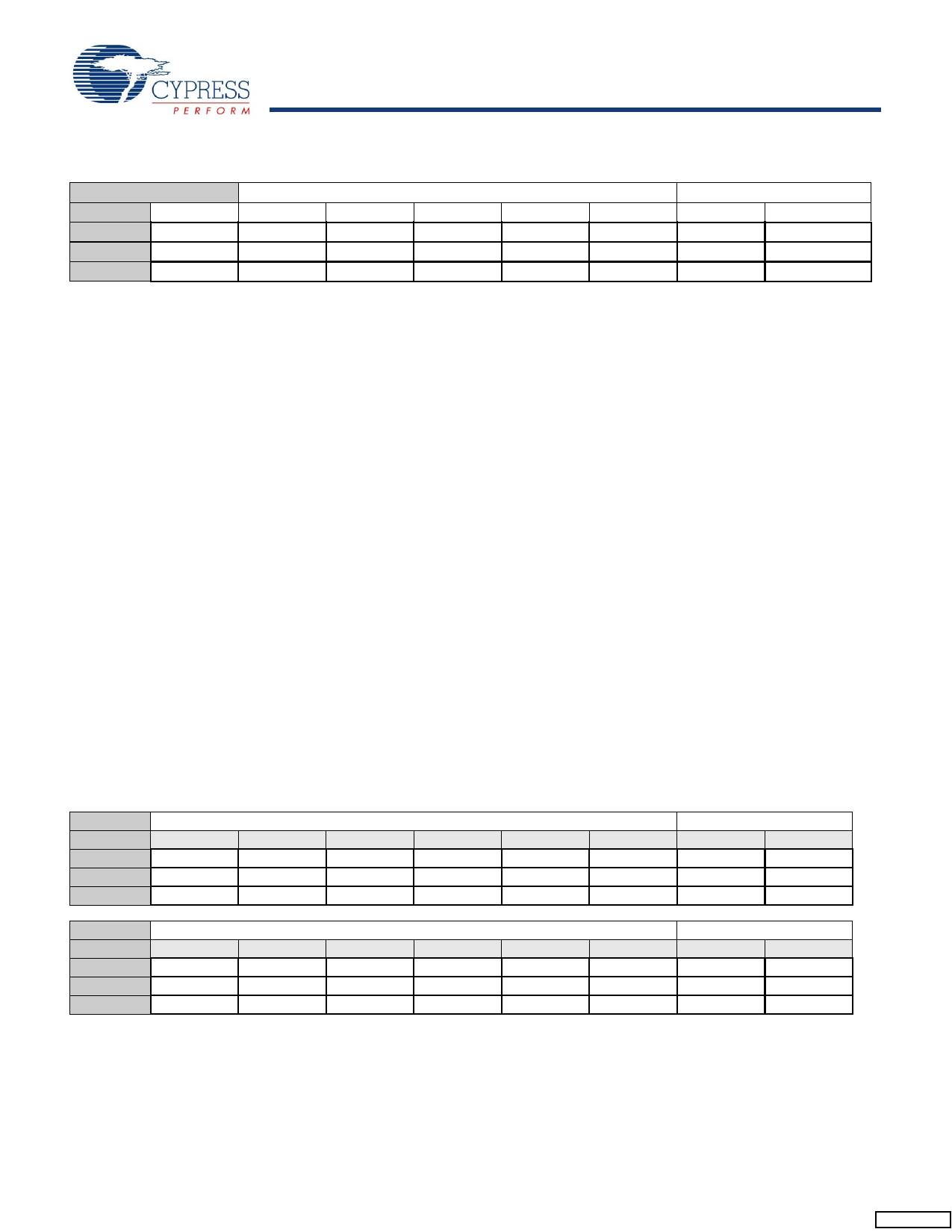
7.4 REVID Register 0x05
These register bits define the silicon revision.
REVID
Bit #
7
Bit
Major
Name
Read/ R/W
Write
Default X
6
Major
R/W
X
5
Major
R/W
X
4
Major
R/W
X
3
2
Minor Minor
R/W R/W
X
X
1
Minor
R/W
X
0x05
0
Minor
R/W
X
The upper nibble is the major revision. The lower nibble is the
minor revision. For example: if REVID = 0x11, then the silicon
revision is 1.1.
7.5 EPxCFG Register 0x06–0x09
These registers configure the large, data-handling SX2
endpoints, EP2, 4, 6, and 8. Figure 3-1 shows the configu-
ration choices for these endpoints. Shaded blocks group
endpoint buffers for double-, triple-, or quad-buffering. The
endpoint direction is set independently—any shaded block
can have any direction.
EPxCFG
Bit #
7
Bit
VALID
Name
Read/ R/W
Write
Default 1
6
5
4
DIR TYPE1 TYPE0
R/W R/W R/W
0
1
0
3
SIZE
2
STALL
0x06, 0x08
1
0
BUF1 BUF0
R/W R/W R/W R/W
0
0
1
0
.
EPxCFG
0x07, 0x09
Bit #
7
6
5
4
3
2
1
0
Bit
VALID DIR TYPE1 TYPE0 SIZE STALL BUF1 BUF0
Name
Read/W R/W R/W R/W R/W R R/W R
R
rite
Default 1
0
1
0
0
0
1
0
7.5.1 Bit 7: VALID
The external master sets VALID = 1 to activate an endpoint,
and VALID = 0 to deactivate it. All SX2 endpoints default to
valid. An endpoint whose VALID bit is 0 does not respond to
any USB traffic.
7.5.2 Bit 6: DIR
0 = OUT, 1 = IN. Defaults for EP2/4 are DIR = 0, OUT, and for
EP6/8 are DIR = 1, IN.
7.5.3 Bit [5,4]: TYPE1, TYPE0
These bits define the endpoint type, as shown in Table 7-3.
The TYPE bits apply to all of the endpoint configuration
registers. All SX2 endpoints except EP0 default to BULK.
Table 7-3. Endpoint Type
TYPE1
0
0
1
1
TYPE0
0
1
0
1
Endpoint Type
Invalid
Isochronous
Bulk (Default)
Interrupt
7.5.4 Bit 3: SIZE
0 = 512 bytes (default), 1 = 1024 bytes.
Endpoints 4 and 8 can only be 512 bytes and is a read only
bit. The size of endpoints 2 and 6 is selectable.
7.5.5 Bit 2: STALL
Each bulk endpoint (IN or OUT) has a STALL bit (bit 2). If the
external master sets this bit, any requests to the endpoint
return a STALL handshake rather than ACK or NAK. The Get
Status-Endpoint Request returns the STALL state for the
endpoint indicated in byte 4 of the request. Note that bit 7 of
the endpoint number EP (byte 4) specifies direction.
7.5.6 Bit [1,0]: BUF1, BUF0
For EP2 and EP6 the depth of endpoint buffering is selected
via BUF1:0, as shown in Table 7-4. For EP4 and EP8 the
buffer is internally set to double buffered and are read only bits.
Table 7-4. Endpoint Buffering
BUF1
BUF0
Buffering
0
0
Quad
0
1
Invalid[10]
1
0
Double
1
1
Triple
Notes:
10. Setting the endpoint buffering to invalid causes improper buffer allocation
Document #: 38-08013 Rev. *E
Page 17 of 42
Share Link: 