HGTG40N60B3 Просмотр технического описания (PDF) - Fairchild Semiconductor
Номер в каталоге
Компоненты Описание
производитель
HGTG40N60B3 Datasheet PDF : 8 Pages
| |||
HGTG40N60B3
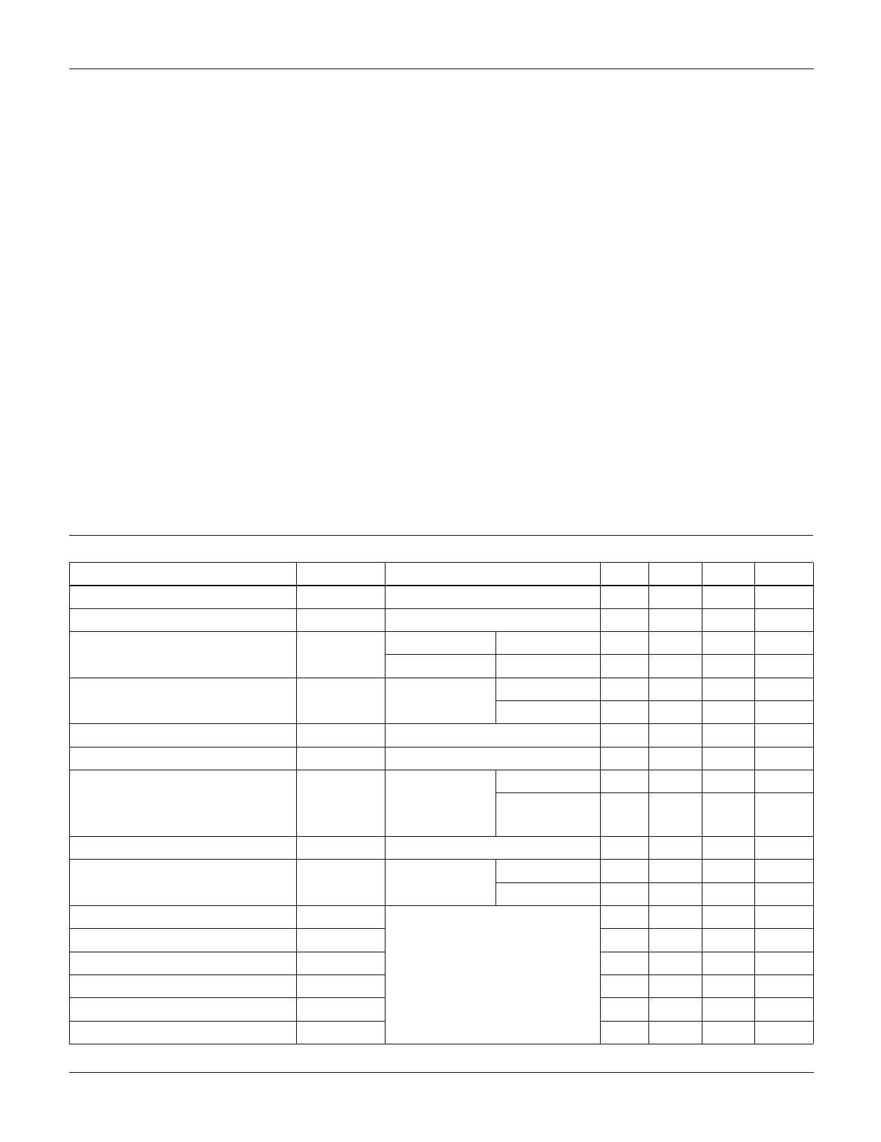
Absolute Maximum Ratings TC = 25oC, Unless Otherwise Specified
HGTG40N60B3
UNITS
Collector to Emitter Voltage . . . . . . . . . . . . . . . . . . . . . . . . . . . . . . . . . . . . . . . . . . . . . .BVCES
Collector Current Continuous
At TC = 25oC . . . . . . . . . . . . . . . . . . . . . . . . . . . . . . . . . . . . . . . . . . . . . . . . . . . . . . . . . IC25
At TC = 110oC . . . . . . . . . . . . . . . . . . . . . . . . . . . . . . . . . . . . . . . . . . . . . . . . . . . . . . . IC110
Collector Current Pulsed (Note 1) . . . . . . . . . . . . . . . . . . . . . . . . . . . . . . . . . . . . . . . . . . . ICM
Gate to Emitter Voltage Continuous. . . . . . . . . . . . . . . . . . . . . . . . . . . . . . . . . . . . . . . . . VGES
Gate to Emitter Voltage Pulsed . . . . . . . . . . . . . . . . . . . . . . . . . . . . . . . . . . . . . . . . . . . .VGEM
Switching Safe Operating Area at TJ = 150oC, Figure 2 . . . . . . . . . . . . . . . . . . . . . . . . SSOA
Power Dissipation Total at TC = 25oC . . . . . . . . . . . . . . . . . . . . . . . . . . . . . . . . . . . . . . . . . PD
Power Dissipation Derating TC > 25oC . . . . . . . . . . . . . . . . . . . . . . . . . . . . . . . . . . . . . . . . . .
Reverse Voltage Avalanche Energy . . . . . . . . . . . . . . . . . . . . . . . . . . . . . . . . . . . . . . . . . EARV
Operating and Storage Junction Temperature Range . . . . . . . . . . . . . . . . . . . . . . . . TJ, TSTG
Maximum Lead Temperature for Soldering . . . . . . . . . . . . . . . . . . . . . . . . . . . . . . . . . . . . . TL
Short Circuit Withstand Time (Note 2) at VGE = 15V. . . . . . . . . . . . . . . . . . . . . . . . . . . . . .tSC
Short Circuit Withstand Time (Note 2) at VGE = 10V. . . . . . . . . . . . . . . . . . . . . . . . . . . . . .tSC
600
70
40
330
±20
±30
100A at 600V
290
2.33
100
-55 to 150
260
2
10
V
A
A
A
V
V
W
W/oC
mJ
oC
oC
µs
µs
CAUTION: Stresses above those listed in “Absolute Maximum Ratings” may cause permanent damage to the device. This is a stress only rating and operation of the
device at these or any other conditions above those indicated in the operational sections of this specification is not implied.
NOTES:
1. Pulse width limited by maximum junction temperature.
2. VCE(PK) = 360V, TJ = 125oC, RG = 3Ω.
S
Electrical Specifications
TC = 25oC, Unless Otherwise Specified
PARAMETER
SYMBOL
TEST CONDITIONS
Collector to Emitter Breakdown Voltage
Emitter to Collector Breakdown Voltage
Collector to Emitter Leakage Current
Collector to Emitter Saturation Voltage
Gate to Emitter Threshold Voltage
Gate to Emitter Leakage Current
Switching SOA
BVCES
BVECS
ICES
VCE(SAT)
VGE(TH)
IGES
SSOA
IC = 250µA, VGE = 0V
IC = -10mA, VGE = 0V
VCE = BVCES
TC = 25oC
VCE = BVCES
TC = 150oC
IC = IC110,
VGE = 15V
TC = 25oC
TC = 150oC
IC = 250µA, VCE = VGE
VGE = ±20V
TJ = 150oC
RG = 3Ω
VGE = 15V
L = 100µH
VCE = 480V
VCE = 600V
Gate to Emitter Plateau Voltage
On-State Gate Charge
Current Turn-On Delay Time
Current Rise Time
Current Turn-Off Delay Time
Current Fall Time
Turn-On Energy
Turn-Off Energy (Note 1)
VGEP
QG(ON)
td(ON)I
trI
td(OFF)I
tfI
EON
EOFF
IC = IC110, VCE = 0.5 BVCES
IC = IC110,
VCE = 0.5 BVCES
VGE = 15V
VGE = 20V
IGBT and Diode Both at TJ = 25oC
ICE = IC110
VCE = 0.8 BVCES
VGE = 15V
RG = 3Ω
L = 100µH
Test Circuit (Figure 17)
MIN
TYP
MAX UNITS
600
-
-
V
20
-
-
V
-
-
100
µA
-
-
6.0
mA
-
1.4
2.0
V
-
1.5
2.3
V
3.0
4.8
6.0
V
-
-
±100
nA
200
-
-
A
100
-
-
A
-
7.5
-
V
-
250
330
nC
-
335
435
nC
-
47
-
ns
-
35
-
ns
-
170
200
ns
-
50
100
ns
-
1050 1200
µJ
-
800
1400
µJ
©2004 Fairchild Semiconductor Corporation
HGTG40N60B3 Rev. B3
Share Link: 