HFA3841 Просмотр технического описания (PDF) - Intersil
Номер в каталоге
Компоненты Описание
производитель
HFA3841 Datasheet PDF : 27 Pages
| |||
Preliminary - HFA3841
PHY Interface
The HFA3841 is intended to support the PRISM family of
Baseband processors with no additional components. This
family currently includes the HFA3860B and HFA3861 DSSS
baseband processors and the other ICs in the PRISM WLAN
chip set. (Other baseband processors may be supported
with custom firmware. See your sales representative for
more information). The HFA3841 interfaces to the HFA386X
baseband processors through two serial interfaces. The
Modem Management Interface (MMI) is used to read and
write internal registers in the baseband processor and
access per-packet PLCP information. The Modem Data
Interface (MDI) provides the receive and transmit data paths
which transfer the actual MPDU data.
Serial Control Port (MMI)
The HFA3841 has a serial port that is used to program the
baseband processor. There are individual chip selects and
shared clock and data lines.
The MMI is used to program the registers and functionality of
the PHY baseband processor.
PHY BASEBAND PROCESSOR
The PHY baseband processor is programmed by HFA3841
firmware.
The PRISM II baseband processor mode works as follows:
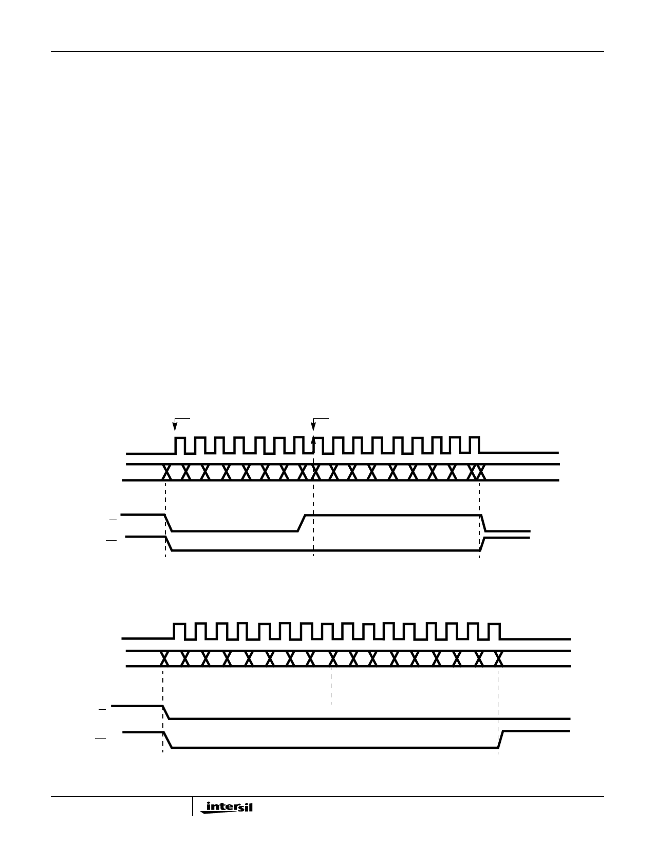
The Control Port consists of 4 signals: SD (serial data),
SCLK (serial clock), R/W (read/write) and CS_BAR (active-
low chip select).
Control Port signaling for read and write operations is
illustrated in Figures 16 and 17 respectively. Detailed timing
relationships appear in Figure 18 and timing specifications
are contained in Table 1.
The BBP always uses the rising edge when clocking data on
the Control Port. This means that when the BBP is receiving
data it uses the rising edge of clock to sample; when driving
data, transitions occur on the rising edge.
Address bits 6 through 1 are significant for selecting
configuration registers. Address bits 7 and 0 are unused.
See the BBP Programming section for register addresses
and suggested values.
For read operations, the rising edge of R/W must occur after
the 7th but prior to the 8th rising edge of SCLK. This ensures
that the first data bit is clocked out of the BBP prior to the
edge used to clock it into the MAC.
For more detailed information on the Control Port and BBP
register programming see the HFA386x data sheets.
SCLK
SD
FIRST ADDRESS BIT
76 5 4 3 2 1
FIRST DATABIT OUT
0 7 65 4 3 21 0
765 432 1
MSB
ADDRESS IN
07 7 6 6 5 4 3 2
MSB
DATA OUT
10
LSB
R/W
CS
FIGURE 16. PRISM II BASEBAND PROCESSOR CONTROL PORT READ TIMING
SCLK
SD
R/W
CS
76 5 4 32 1 07 6 54 3 2 10
76 5 4 3 21 0 765 4 3 21 0
MSB
ADDRESS IN
MSB
DATA IN
LSB
FIGURE 17. PRISM II BASEBAND PROCESSOR SERIAL CONTROL PORT WRITE TIMING
20
Share Link: 