HFA3841 Просмотр технического описания (PDF) - Intersil
Номер в каталоге
Компоненты Описание
производитель
HFA3841 Datasheet PDF : 27 Pages
| |||
Preliminary - HFA3841
buffer access path) will result in the pre-read data
becoming invalidated.
• If another read cycle has invalidated the pre-read, then a
memory arbitration delay will occur on the next buffer
access path read cycle.
HIREQ-
Immediately after reset, the HIREQ- signal serves as the
RDY/BSY (per the PC Card standard). Once the HFA3841
firmware initialization procedure is complete, HIREQ- is
configured to operate as the interrupt to the PC Card socket
controller. Both Level Mode and Pulse Mode interrupts are
supported. By default, Level mode interrupts are used, so
the interrupt source must be specifically acknowledged or
disabled before the interrupt will be removed.
HRESET
When reset is removed, the CIS table is initialized and, once
complete, HIREQ- is set high (HIREQ- acts as RDY/BSY
from reset and is set high to indicate the card is ready for
use). The CIS table resides in Flash memory and is copied
to RAM during firmware initialization. The host system can
then initialize the card by reading the CIS information and
writing to the configuration register.
ISA PnP
The HFA3841 can be connected to the ISA bus and operate
in a Plug and Play environment with an additional chip such
as the Fujitsu MB86703, Texas Instruments TL16PNP200A,
or Fairchild Semiconductor NM95MS15. See the Application
Note AN9874, "ISA Plug and Play with the HFA3841" for
more details.
Register Interface
The logical view of the HFA3841 from the host is a block of
32 word wide registers. These appear in IO space starting at
the base address determined by the socket controller. There
are three types of registers.
HARDWARE REGISTERS (HW)
• 1 to 1 correspondence between addresses and registers.
• No memory arbitration delay, data transfer directly to/from
registers.
• AUX base and offset are write-only, to set up access
through AUX data port.
• Note: All register cycles, including hardware registers,
incur a short wait state on the PC Card bus to insure the
host cycle is synchronized with the HFA3841's internal
MCLK.
MEMORY MAPPED REGISTERS IN DATA RAM (MM)
• 1 to 1 correspondence.
• Requires memory arbitration, since registers are actually
locations in HFA3841 memory.
• Attribute memory access is mapped into RAM as Base-
address + 0x400.
• AUX port provides host access to any location in HFA3841
RAM (reserved).
BUFFER ACCESS PATH (BAP)
• No 1 to 1 correspondence between register address and
memory address (due to indirect access through buffer
address pointer registers).
• Auto increment of pointer registers after each access.
• Require memory arbitration since buffers are located in
HFA3841 memory.
• Buffer access may incur additional delay for Hardware
Buffer Chaining.
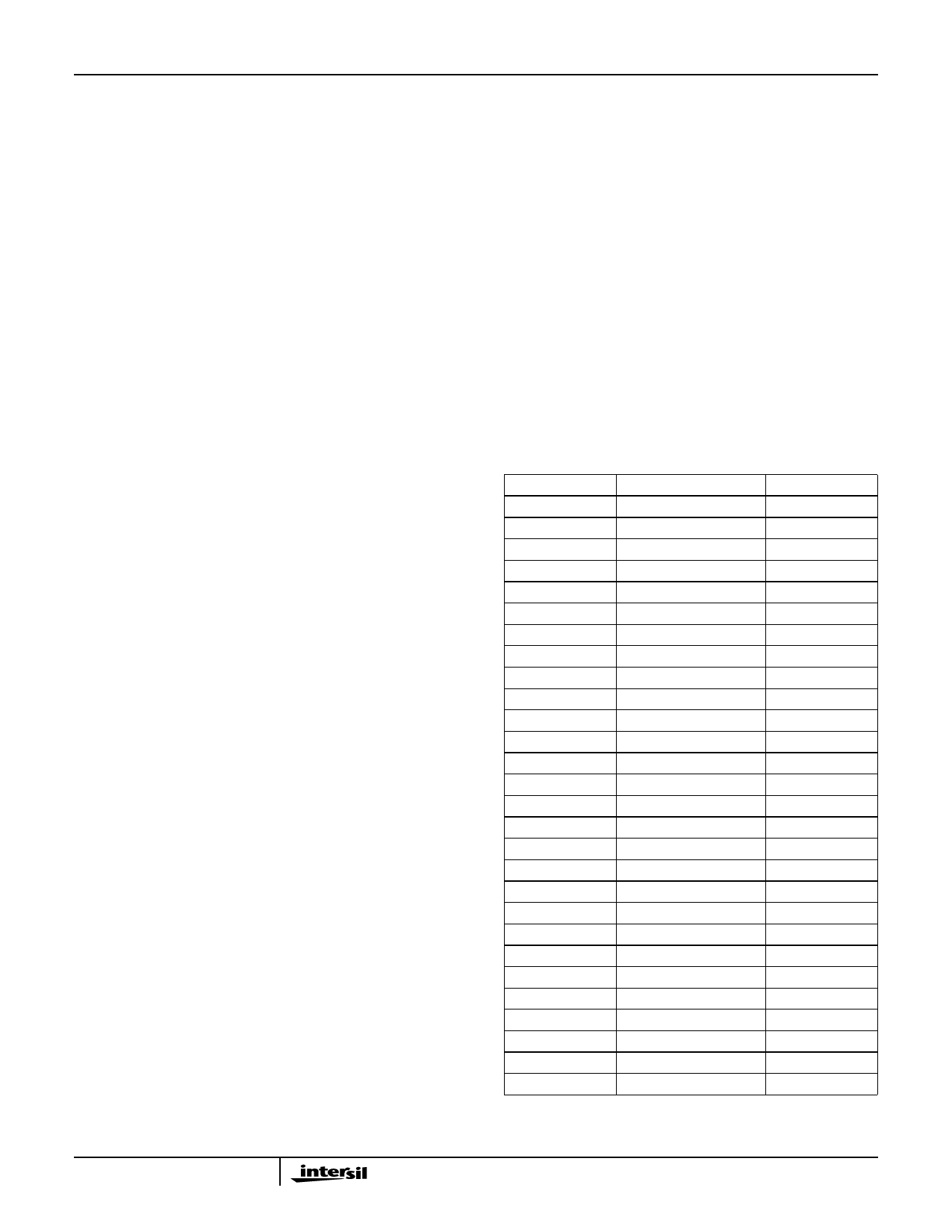
I/O OFFSET
00
02
04
06
08
0A
0C
0E
10
20
22
24
18
1C
36
1A
1E
38
30
32
34
14
28
2A
2C
3A
3C
3E
NAME
Command
Param0
Param1
Param2
Status
Resp0
Resp1
Resp2
InfoFID
RxFID
AllocFID
TxComplFID
BAP Select0
BAP Offset0
BAP Data0
BAP Select1
BAP Offset1
BAP Data1
EvStat
IntEn
EvAck
Control
SwSupport0
SwSupport1
SwSupport2
AuxBase
AuxOffset
AuxData
TYPE
MM
MM
MM
MM
MM
MM
MM
MM
MM
MM
MM
MM
MM
MM
BAP
MM
MM
BAP
HW
HW
HW
MM
MM
MM
MM
HW
HW
(reserved)
18
Share Link: 