HI1260JCQ Просмотр технического описания (PDF) - Intersil
Номер в каталоге
Компоненты Описание
производитель
HI1260JCQ Datasheet PDF : 13 Pages
| |||
HI1260
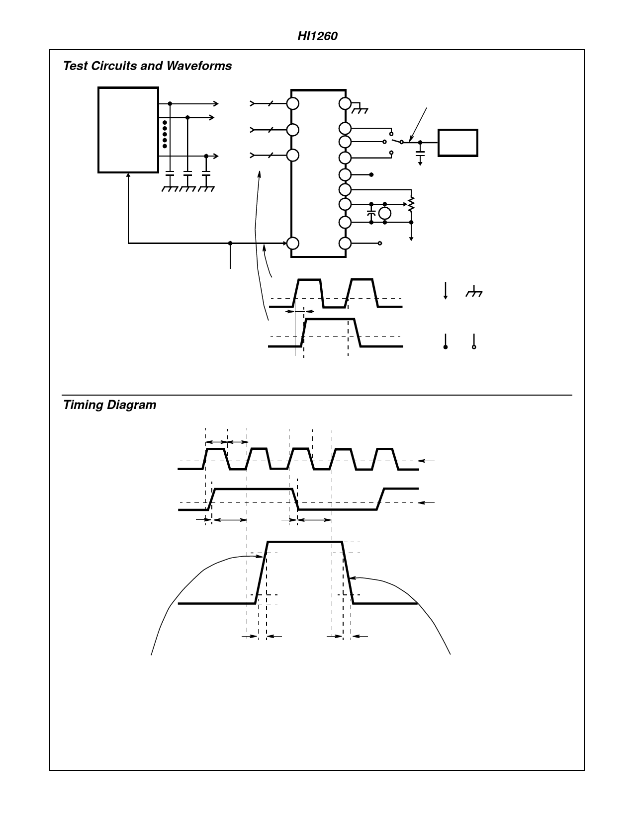
Test Circuits and Waveforms (Continued)
8-BIT
COUNTER
(TTL OUTPUT)
(MSB)
OUT D1
D2
(LSB)
D8
IN
100PF
MCLK
f = 1 MSPS
TTL LEVEL
RECTANGULAR
WAVE
D1 -D8
8 (R)
D1 -D8
8 (G)
D1 -D8
8 (B)
39 - 42
44 - 47
1-8
9 - 16
18
CLK
HI1260
CLK
19, 37, 43
DIGITAL RAMP WAVEFORM GENERATION
ROUT
33
GOUT
31
BOUT
29
27
VREF
25 VSET
24
3K
+
-
V
23
33µF
20
AGND DGND
D1 TO D8
5ns TO 300ns
AVCC DVCC
Timing Diagram
CLK
DATA
D/A OUT
TIMING OF CLK AND DATA
FIGURE 6. GLITCH ENERGY TEST CIRCUIT
t1 t12 t2
tPW1 tPW0
tX
t3 t34 t4
tY
tH
tS
tH
100%
tS
90%
VTH = 1.5V
VTH = 1.4V
0%
10%
VTH: THRESHOLD LEVEL
10%
0%
90%
100%
tr
At the time t = tx, the data of individual bits are
switched and thereafter, when the CLK becomes L →
H at t = t2, the D/A OUT is varied synchronous with it.
That is, the D/A OUT is synchronous with the rise of
the CLK. (In this case, fetching of the data is carried
out at the fall of the CLK (at the time when t = T12).)
tf
At the time t = TY, the data of individual bits are
switched and thereafter, when the CLK becomes L →
H at t = t4, the D/A OUT is synchronous with it. That
is, the D/A OUT is synchronous with the rise of the
CLK. (In this case, fetching of the data is carried out
at the fall of CLK (at the time when t = t4).)
FIGURE 7.
10-9
Share Link: 