CXA2016S Просмотр технического описания (PDF) - Sony Semiconductor
Номер в каталоге
Компоненты Описание
производитель
CXA2016S Datasheet PDF : 12 Pages
| |||
CXA2016S
Pin
Pin
Symbol
No
voltage
7 Video IN —
8 HD SEL —
9
ISC
1.2 V
10
ISJ
1.2 V
11 GND
0V
12 VSS REF 3.125 V
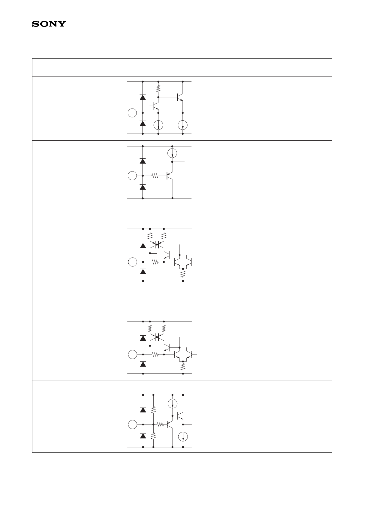
Equivalent circuit
VCC
2k
7
GND
VCC
8
1k
GND
VCC
2k 1k
9
100
50k
GND
VCC
4k 1k
10
100
—
12k
12
1k
20k
50k
GND
VCC
GND
Description
Inputs sync on video (sync at negative
polarity). Connects in series a 1 µF
capacitor and a 270 Ω resistance to
input signals.
Selects output processing of HD
(H. Drive Pulse) at a VD interval.
Input at TTL level.
When Low level is selected, HD is not
output at a VD interval.
When High level is selected, HD is
output at the VD interval.
Resistance connecting pin for
reference current source of clamp
pulse output circuit, and connects 12
kΩ resistance to GND. When a 12 kΩ
resistance is connected, a 100 µA
current flows through this pin (pulse
width is approximately 300 ns).
Clamp pulse output pulse width is
varied by changing the value of the
resistance.
∗Use a metal film resistor with an
accuracy of ±1 %
Resistance connecting pin for
reference current source and
connecting 12 kΩ resistance to GND.
When the resistance is connected, a
100 µA current flows through this pin.
∗Use a metal film resistor with an
accuracy of ±1 %
GND pin.
Reference pin for V. sync separator of
composite sync and video sync.
—3—
Share Link: 