ADP3810AR-12.6 Просмотр технического описания (PDF) - Analog Devices
Номер в каталоге
Компоненты Описание
производитель
ADP3810AR-12.6 Datasheet PDF : 14 Pages
| |||
ADP3810/ADP3811
battery voltage is at least 1.5 V with a programmed charge cur-
rent of 0.1 A. For a higher programmed charge current, the
battery voltagecan drop below 1.5 V, and Vee is stilI maintained
above 2.7 V. This is because of the additional energy in the
flyback transformer, which transfers more energy through the
10 nF capacitor to Vee. The 22 ~ bypass capacitor on Vee
stores the energy transferred through the 10 nF capacitor.
The Battery Charge Current vs. Battery Voltage characteristics
for four different charge current settings are given in Figure 24.
The high gain of the internal amplifiers ensures the sharp transi-
tion between current mode and voltage mode regardless of the
charge current setting. The fact that the current remains at full
charging until the battery is very close to its final voltage ensures
fast charging times.
Secondary Side Component Calculations
Design Criteria:
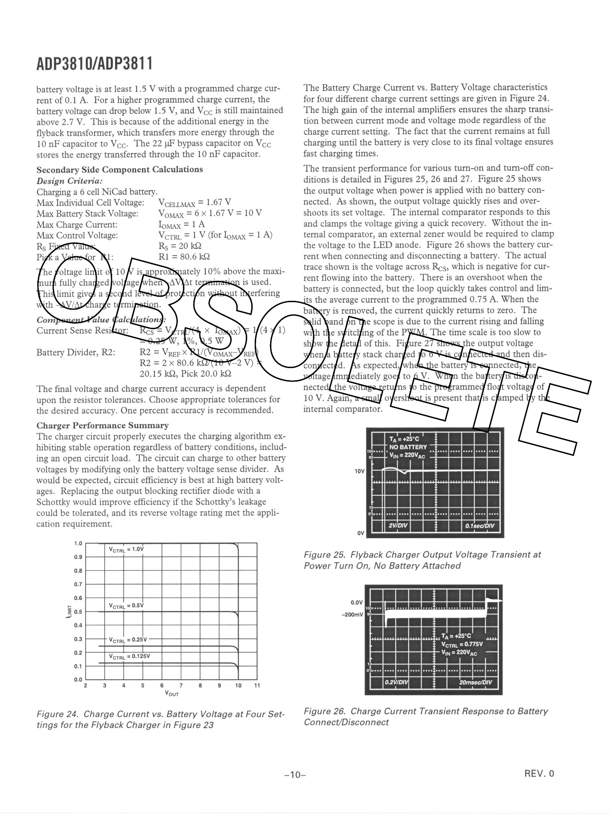
The transient performance for various turn-on and turn-off con-
ditions is detailed in Figures 25, 26 and 27. Figure 25 shows
Charging a 6 cell NiCad battery.
the output voltage when power is applied with no battery con-
= Max Individual Cell Voltage: VeElLMAX 1.67 V
nected. As shown, the output voltage quickly rises and over-
= = Max Battery Stack Voltage: VOMAX 6 x 1.67 V 10 V
shoots its set voltage. The internal comparator responds to this
= Max Charge Current:
= = Max Control Voltage:
= Rs FixedValue:
= Picka Valuefor Rl:
10MAX 1A
VeTRL 1 V (for IoMAX 1 A)
Rs 20 k.Q
Rl 80.6 k.Q
The voltage limit of 10 V is approximately 10% above the maxi-
mum fully charged voltage when -!:N/l1t termination is used.
This limit gives a second level of protection without interfering
Owith -I1V/l1tcharge termination.
Component Value Calculations:
B= = Current Sense Resistor: Res VeTRLI(4 x 10MAx) 1/(4 xl)
= = S0.25 W, 1%, 0.5 W
O= Battery Divider, R2:
R2 = VREFXR1/(VOMAX-VREF)
R2 2 x 80.6 k.Q/(lOV-2 V)
20.15 kQ, Pick 20.0 k.Q
L The final voltage and charge current accuracy is dependent
E upon the resistor tolerances. Choose appropriate tolerances for
the desired accuracy. One percent accuracy is recommended.
TE Charger Performance Summary
and clamps the voltage giving a quick recovery. Without the in-
ternal comparator, an external zener would be required to clamp
the voltage to the LED anode. Figure 26 shows the battery cur-
rent when connecting and disconnecting a battery. The actual
trace shown is the voltage across Res, which is negative for cur-
rent flowing into the battery. There is an overshoot when the
battery is connected, but the loop quickly takes control and lim-
its the average current to the programmed 0.75 A. When the
battery is removed, the current quickly returns to zero. The
solid band on the scope is due to the current rising and falling
with the switching of the PWM. The time scale is too slow to
show the detail of this. Figure 27 shows the output voltage
when a battery stack charged to 6 V is connected and then dis-
connected. As expected, when the battery is connected, the
voltage immediately goes to 6 V. When the battery is discon-
nected, the voltage returns to the programmed float voltage of
10 V. Again, a small overshoot is present that is clamped by the
internal comparator.
The charger circuit properly executes the charging algorithm ex-
hibiting stable operation regardless of battery conditions, includ-
ing an open circuit load. The circuit can charge to other battery
! TA=+25°C
00.... NO BATTERY .... .... .... .... ....
9=; 'V,N=220VAC..
voltages by modifying only the battery voltage sense divider. As
10V
would be expected, circuit efficiency is best at high battery volt-
ages. Replacing the output blocking rectifier diode with a
Schottky would improve efficiency if the Schottky's leakage
could be tolerated, and its reverse voltage rating met the appli-
10
o...
.... .... .... .... .... .... .... .... ....
cation requirement.
2VIDIV
OV
O.I..seclDIV
1.0
VCTRL = 1.0V
0.9
Figure 25. Flyback Charger Output Voltage Transient at
0.8
Power Turn On, No Battery Attached
0.7
0.6
....
J 0.5
0.4
0.3 -
0.2
VCTRL= 0.5V
I
I .J.
VCTRL =0.25V
I
VCTRL=0.125V
0.1
II
0.0 -
234
6 78
Your
10 11
O.OV 10 .... ....... ........ .... .... ........ ....
-200mV 9
TA=+25°C II:
VCTRL = O.775V
V,N=220VAC -==
0
II n II
"I ,... .... .... .... .... .... .... .... .... ....
O.2V1DD!I
20mseclDIV
Figure 24. Charge Current vs. Battery Voltage at Four Set-
tings for the Flyback Charger in Figure 23
Figure 26. Charge Current Transient Response to Battery
Connect/Disconnect
-10-
REV. 0
Share Link: 