MSM62X42B Просмотр технического описания (PDF) - Oki Electric Industry
Номер в каталоге
Компоненты Описание
производитель
MSM62X42B Datasheet PDF : 27 Pages
| |||
¡ Semiconductor
MSM62X42B
PIN DESCRIPTION
D0 to D3 (Data buses 0 to 3)
Data input/output pins to be directly connected to a microcomputer data bus for reading
and writing of the register controlled by the microcomputer. The interface serves as positive
logic and CS0=L, 1=H, RD=L, and as output mode when WR=H. It becomes high impedance
except these cases.
A0 to A3 (Address buses 0 to 3)
These are input pins to be directly connected to a microcomputer address bus for register
assignment which is read and written by a microcomputer. These address data are used in
combination with ALE for addressing registers.
ALE (Address Latch Enable)
This is an input pin to read address data and CS0.
The address bus andCS0 are read into a IC when ALE="H". The address data in the case of
ALE=L in the IC is held. CS1 functions to ALE independently.
When the microcomputer of MSC-48, 51 or 80 system having an ALE output is used, this pin
is connected to the ALE output of the microcomputer. When 4 Bits of A0 to A3 in a 4 Bit
microcomputer are commonly used with an another peripheral IC. When the microcom-
puter does not have the ALE output, the ALE input of this IC is fixed to "H".
WR (WRITE)
This is a input pin for which the data is written into this IC by a microcomputer. When
CS1=H, D0 ~ D3 data are written into the designated registers by A0 to A3 and ALE at the
rising edge of WR.
RD (READ)
This is an input pin to read this IC data by a microcomputer. When CS1=H, RD outputs the
register data designated by A0 to A3 and ALE during "L". If both WR and RD are set at "L",
this should be inhibited because it becomes the cause for malfunction.
CS0, CS1(Chip Select 0•1)
These pins enable/disable ALE, RD and WR operation, when CS1=H at CS0=L, these pins
become effective. In other combination except this, the pins become equivalent to ALE=L
and WR=RD=H unconditionally in the IC internal. However, CS0 needs operation related
with ALE, while CS1 works independently to ALE. CS1 must be connected to the power
supply voltage detector. Refer to the item, “CS1 of APPLICATION NOTE”.
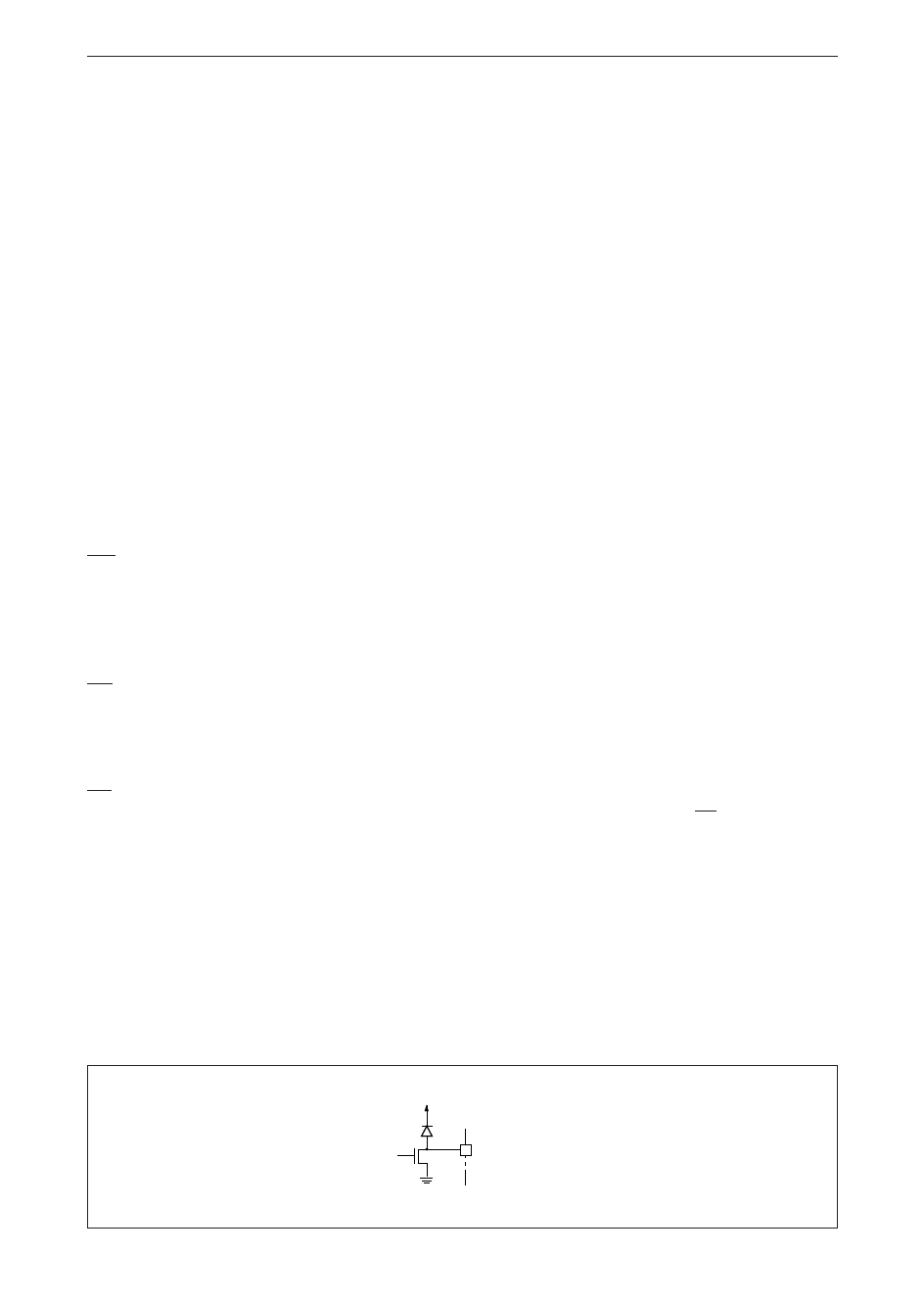
STD • P (STANDRD Pulse)
Output pin of N-CH OPEN DRAIN type. The output data is controlled by the D1 data
content of CE register. This pin has a priority to CS0 and CS1. Refer to the item "CE REGISTER
FOR FUNCTIONAL DESCRIPTION OF REGISTERS".
VDD
N-CH
STD.P Output
51
Share Link: 