MSM62X42B Просмотр технического описания (PDF) - Oki Electric Industry
Номер в каталоге
Компоненты Описание
производитель
MSM62X42B Datasheet PDF : 27 Pages
| |||
¡ Semiconductor
MSM62X42B
f) Regarding W
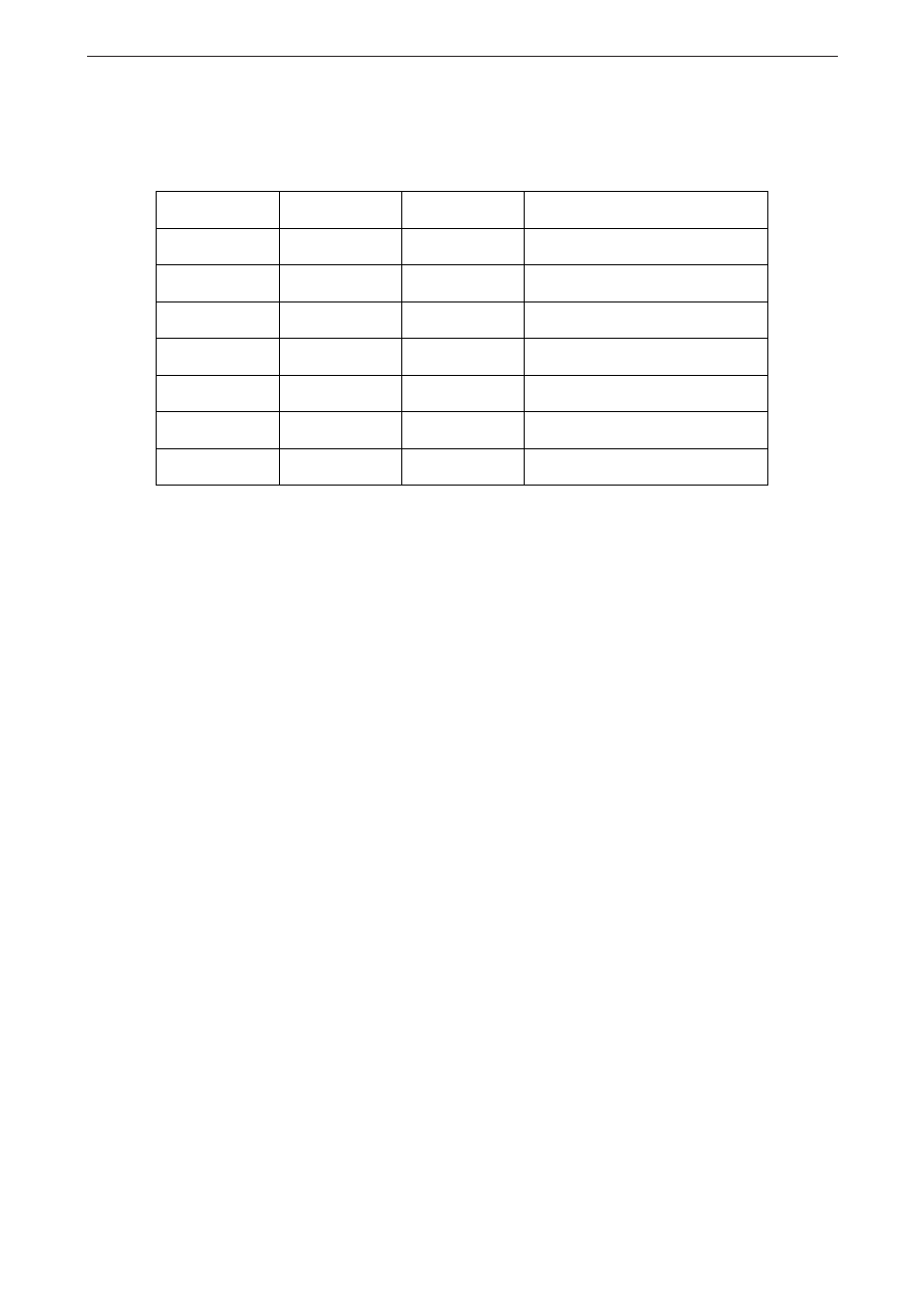
The Register W data limits are up-counted from 0 to 6. The following Table 1 shows a possible
data definition.
TABLE 1
W4
W2
W1
Day of Week
0
0
0
Sunday
0
0
1
Monday
0
1
0
Tuesday
0
1
1
Wednesday
1
0
0
Thursday
1
0
1
Friday
1
1
0
Saturday
CD REGISTER (Control D Register)
a) HOLD (D0)
• This Register is one means used for reading out registers S1 to W (addresses 0 to C) and
a bit used for writing. "1" bit to this bit is written and when BUSY bit shows "0", the clock
more than 1 second digit stops and the reading and writing become possible (Refer to the
item APPLICATION NOTE for reading which does not use HOLD bit). When BUSY was
"1" and after reading have finished, "0" is written to HOLD bit. If the writing of "0" is
omitted, then this results in the cause for erroneous data. Setting this bit to "1" inhibits
a carry to 1 second counter in the IC internal, but a carry to a second counter caused during
the duration of "1" is automatically compensated (+1 second) by only one time at the time
when "0" is written to this bit. However, the carry after the second is disregarded and is
not compensated (loss second).
• If CS1 makes "L", the HOLD bit becomes equivalent to the writing to "0" and becomes "0".
b) BUSY (D1)
• The status bit in the IC internal which shows the interface condition with a microcom-
puter. When the registers S1 to W (addresses 0 to C) is written, when HOLD bit is always
"1" and when BUSY bit is surely "0", in case the HOLD bit is used for reading, this is
performed when the BUSY bit is "0". "0" of the BUSY bit continues while the HOLD bit
is "1". When the HOLD bit makes "0", the BUSY bit becomes "1".
• The operation for the registers CD, CE and CF is irrespectively performed for the HOLD
bit and BUSY bit.
• The BUSY bit is "1" uncondiotinally when the HOLD bit=0 and when "1" written into the
HOLD bit, BUSY or not BUSY can be confirmed and when BUSY="1", "0" is once written
into the HOLD bit, and then "1" is again written. BUSY is checked. The routine procedure
like this [HOLD ¨ "0", HOLD ¨ "1", BUSY check] is repeated, or after "0" is written into
the HOLD bit, "1" is again written into the HOLD bit after 190µs and BUSY=0 is
confirmed.
• The time when this IC is BUSY is 190µs per one second
• The writing into the BUSY bit cannot be performed.
53
Share Link: 