UT1750AR12WCC Просмотр технического описания (PDF) - Aeroflex UTMC
Номер в каталоге
Компоненты Описание
производитель
UT1750AR12WCC Datasheet PDF : 56 Pages
| |||
The advanced architecture of the UT1750AR allows the system
designer to define RISC macros accessible through the MIL-
STD-1750A Built-In Function (BIF) opcode. These user-
defined RISC macros can be any regularly-used function
requiring the UT1750AR’s high-speed, real-time processing
capabilities. The UT1750AR fetches the BIF instruction from
Operand memory just like any other 1750 instruction; it then
decodes the BIF. The resulting UT1750AR-generated RISC
address points to the location of the user-defined macro in RISC
memory. RISC macro execution proceeds just as it would for
any other 1750 instruction. MIL-STD-1750A permits the
system designer to define up to 256 BIF variations.
REGISTER ARCHITECTURE
The UT1750AR has a register-oriented architecture (figure 1).
The registers within the UT1750AR fall into two categories:
general purpose registers, and specialized registers. All the
UT1750AR’s registers are accessible to the programmer
through the RISC instruction set. The programmer uses data
from these registers to perform arithmetic and logical functions,
alter program flow, detect various system and processor faults,
determine processor status, provide control for UART and timer
functions, and provide interrupt processing and exception-
handling control.
16 BITS 16 BITS
CONCATENATED 32-BIT
REGISTER PAIR
R0
R1
XR0
R2
R3
XR2
R4
R5
XR4
R6
R7
XR6
R8
R9
XR8
R10
R11
XR10
R12
R13
XR12
R14
R15
XR14
R16
R17
XR16
R18
R19
XR18
ACCUMULATOR
ACC
Figure 6. General Register Set
General Purpose Registers
Figure 6 shows the UT1750AR’s 20 general purpose registers.
All RISC instructions use these registers; any register or register
pair can be either the source or the destination for any RISC
instruction. The UT1750AR normally accesses these registers
as single-word 16-bit registers although the UT1750AR can
concatenate these registers into 32-bit double-word register
pairs. When the programmer uses the general purpose registers
as a double-word register pair, the most significant 16 bits of
the 32-bit words are stored in the even-numbered register of the
register pair. For instance, if a 32-bit word is stored in Register
Pair XR6, the most significant word is stored in register R6 and
the least significant word is stored in register R7.
In addition to the 20 general purpose registers, the UT1750AR
has a 32-bit Accumulator (ACC). The ACC is normally a
destination register, although under certain circumstances it can
be the source register. The Accumulator retains the most
significant half of the product during a multiply instruction or
the remainder during a divide operation.
Specialized Registers
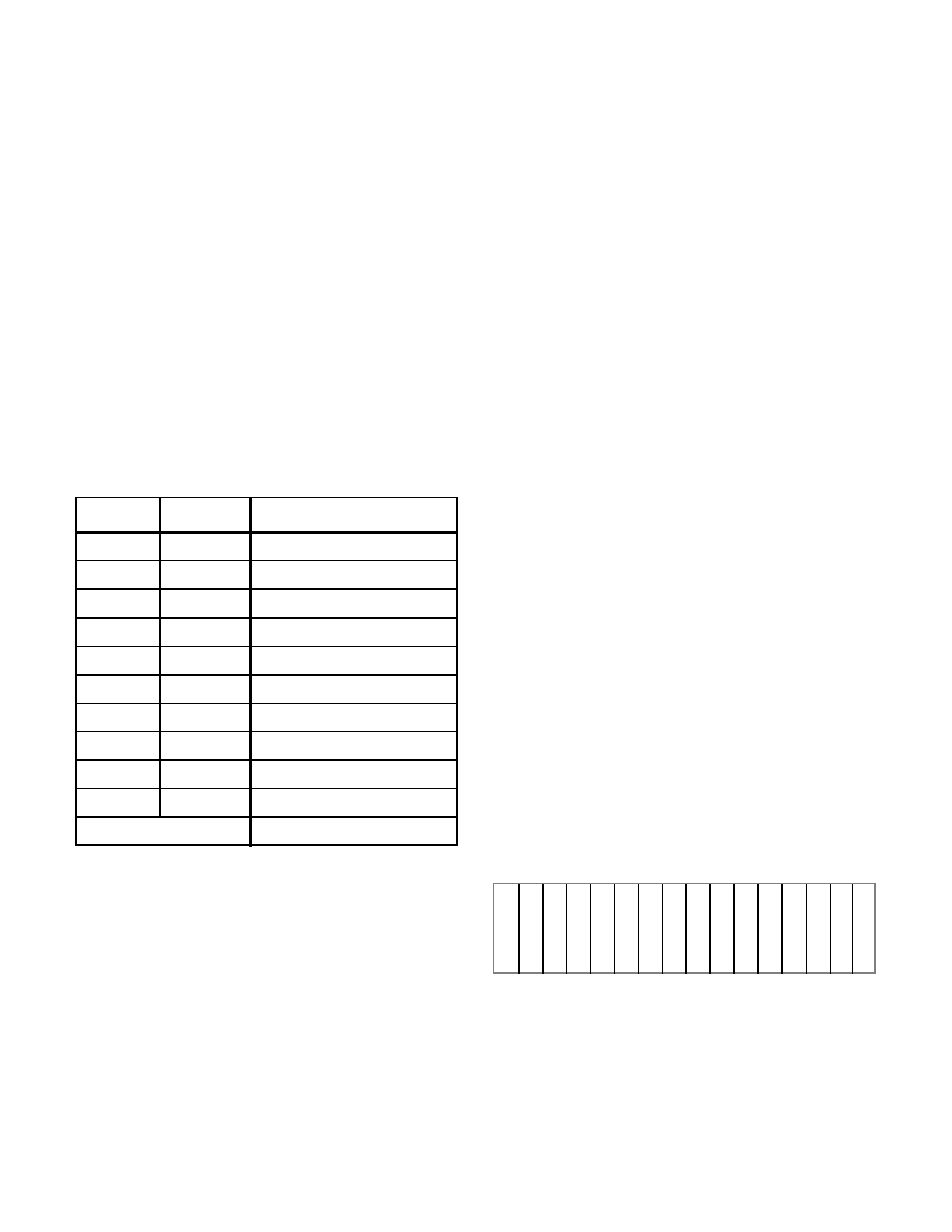
The UT1750AR has 16 special purpose registers (figures 7
through 24). The values in the brackets indicate the power-up
condition. They are:
1. Stack Pointer Register (SP) [XXXX16]
2. System Status Register (STATUS)
3. UART Receiver Buffer Register (RCVR)
[XX0016]
4. UART Transmitter Buffer Register (TXMT)
[XX0016]
5. Pending Interrupt Register (PI) [000016]
6. Fault Register (FT) [000016]
7. Interrupt Mask Register (MK) [XXXX16]
8. 1750 Status Register (SW) [000016]
9. RISC Instruction Counter Register (IC)
[0000016]
10. RISC Instruction Counter Save Register (ICS)
[XXXXX16]
11. RISC Instruction Register (IR) [000016]
12. 1750 Pipeline Register (PIPE) [XXXX16]
13. 1750 Program Register (PR) [XXXX16]
14. 1750 Program Counter (PC) [XXXX16]
15. 1750 Timer A Register (TA) [000016]
16. 1750 Timer B Register (TB) [000016]
The RISC instruction set provides access to most of the special
purpose registers.
The Stack Pointer Register
Figure 7. The UT1750AR uses the 16-bit Stack Pointer Register
as an address pointer on Push and
15 14 13 12 11 10 9 8 7 6 5 4 3 2 1 0
S S SSSSS SSS SSSSSS
P P PPPPP PPP PPPPPP
1 1 11119 876 543210
5 43210
MSB
LSB
Figure 7. The Stack Pointer Register (SP)
14
Share Link: 