MM1292KF Просмотр технического описания (PDF) - Mitsumi
Номер в каталоге
Компоненты Описание
производитель
MM1292KF Datasheet PDF : 7 Pages
| |||
MITSUMI
Protection of Lithium Ion Batteries (two cells in series) MM1292
When the cell voltage of either the H or L cell exceeds VALM, an overcharge detection signal is output to the
data intake section, and a reset signal is prohibited from going to the data processing section.
When more than two consecutive clocks of the excess charging detection signal are input to the data intake
section, a determination is made that the overcharging detection signal has been properly input, and it is
output to the next stage. This prevents noise and mistaken determinations of overcharging caused by excess
cell voltage fluctuation.
When the date intake section outputs the overcharging detection signal, the data charge section goes into
operation. When more than two clocks of overcharging signals are input, this activates the latch on the
overcharging signal.
When the overcharging signal latch in the date latch section is activated, the next non-induction time circuit
goes into operation. When this operates, the TD pin is charged by constant current (ITC). The TD pin potential
and the threshold value (VTC) are compared by the non-induction time circuit comparator. When TD pin
voltage exceeds VTC, the OC pin output stage becomes operable and OC pin output PNP-TR (open collector)
is switched on. Also, bias current is supplied to the timing generation circuit and the operation of the
overcharging detection circuit is maintained.
When discharge occurs during overcharge mode (GND < DS pin), the discharge detection circuit charges the
TD pin and non-induction time is reset.
When cell voltage falls below VALM and the overcharging detection circuit signal is off, the reset prohibition is
lifted. The reset signal is sent to the data intake and data latch sections and the non-induction time circuit,
and normal mode is reinstated.
A diode is built in between the OC pin and GND. When OC pin potential falls below GND terminal VF, current
flows from the OC pin.
Therefore, when battery pack voltage <<charging voltage (charging device), charging is immediately
prohibited. (Generation conditions for the above mode vary depending on the external constant.)
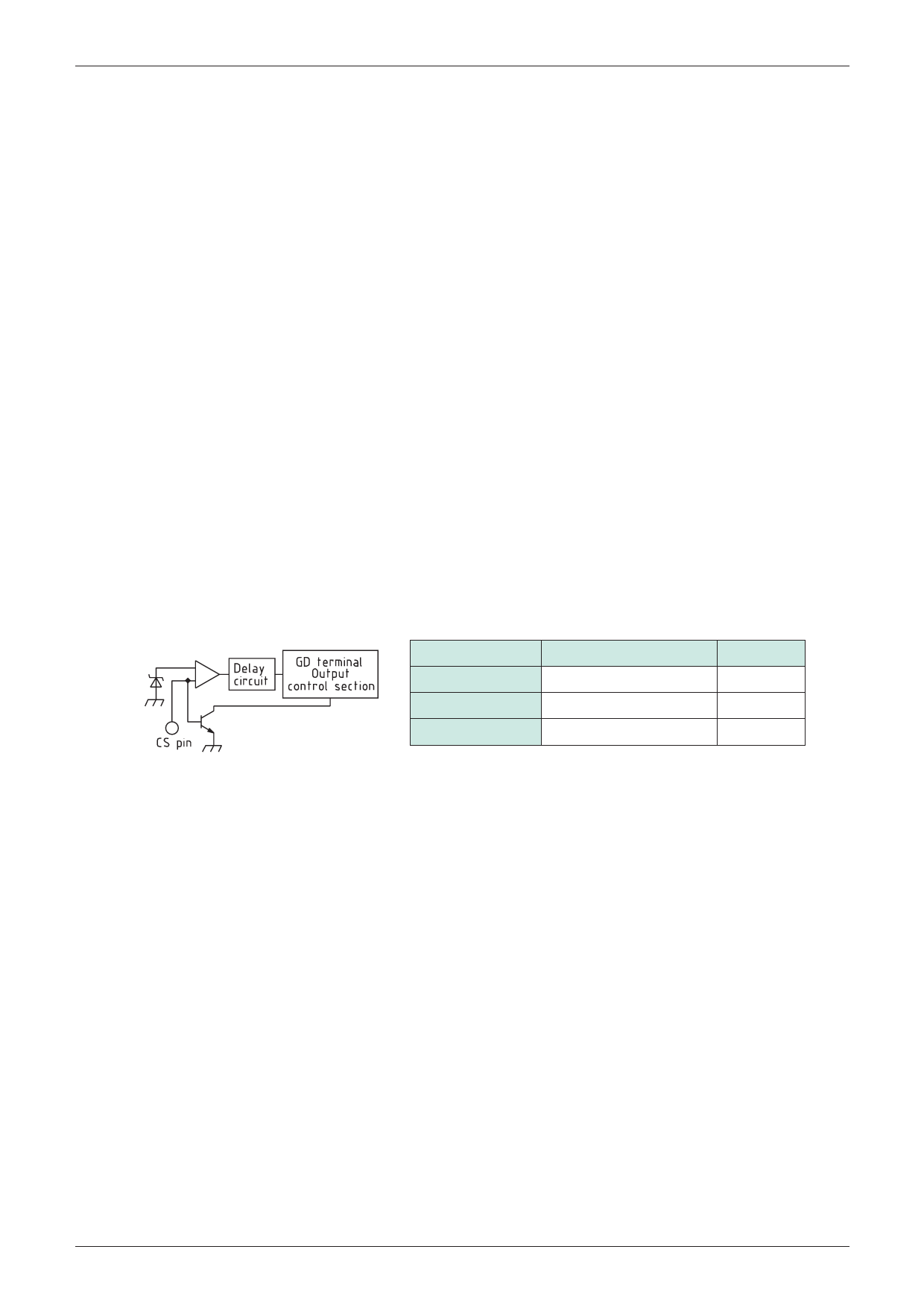
3. Overcurrent Detection Circuit
CS-GND Voltage
Mode
Delay Time
Below VCS
Normal Mode
-
VCS~VF
Overcurrent Mode (Normal) tOC1
Above VF Overcurrent Mode (Short) tOC2
(VF : Voltage between built-in NPN-TR and base emitter)
The overcurrent detection circuit operates during overcharging. Load current detects current flowing on FET
equivalently, by monitoring the voltage between discharge control FET drain sources using the voltage
between CS-GND. (Monitoring of voltage drop using FET ON resistor load current.)
There are two modes for overcurrent detection : the normal mode and the short mode.
In normal mode, when voltage between CS-GND is equal to that between VCS-Vf, overcharging detection
output at this time is input to the internal delay circuit. When overcurrent detection continues for longer than
overcurrent delay time 1 (tOC1), overcurrent mode is activated, and GD pin output goes L. (Discharge control
FET ON)
In short mode, when the voltage between CS-GND exceeds VF, the overcurrent mode operates without going
through the delay circuit. The delay time is determined by the internal circuit operating speed (Overcurrent
delay time 2 [tOC2], so the flow of overcurrent to the discharge control FET is for a short duration, limiting
stress on the FET.)
The VF has a temperature factor of-2mV/(C, so the switching level between normal and short mode varies
with the ambient temperature.
The overcurrent detection voltage (VCS) is fixed, so the current value for overcurrent detection changes
according to discharge control FET ON resistance. Therefore, select an FET that conforms to the detection
current. FET ON resistance is highly sensitive to temperature, due to overcurrent detection voltage, and the
detection current changes due to FET heat emission resulting from ambient temperature and load current. In
addition, users should be aware that FET ON resistance also changes due to the voltage between FET gate
sources. (ON resistance rises when the voltage between gate sources falls.)
Load release resets from overcurrent mode.
Share Link: 