MM1292KF Просмотр технического описания (PDF) - Mitsumi
Номер в каталоге
Компоненты Описание
производитель
MM1292KF Datasheet PDF : 7 Pages
| |||
MITSUMI
Applications
1. Cellular phones
2. Movies
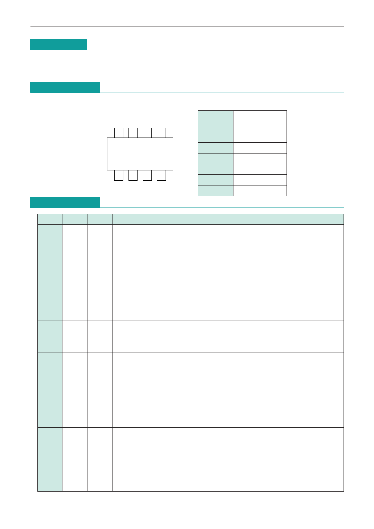
Pin Assignment
Protection of Lithium Ion Batteries (two cells in series) MM1292
8765
Pin Description
1234
SOP-8C/SOP-8D
1
OC
2
GD
3
N.C
4
GND
5
TD
6
VL
7
CS
8
VH
Pin No.
1
2
3
4
5
6
7
8
Pin
OC
GD
DS
GND
TD
VL
CS
VH
Output
Function
Output pin for control of the charging control FET. When voltage detected between
VH-VL or VL-GND goes over overcharge detection voltage (VALM), the output PNP-
Output TR (open collector output) is switched ON, and charging is prohibited by activating
the element (NPN-TR, or N-ch FET) that switches the charging control FET to OFF.
This operation continues until the voltage falls below VALM.
Output pin for driving the discharge control FET. When voltage detected between VH-
VL and VL-GND goes over excess discharge voltage (VS), this pin goes H. When
Output
voltage detected between VH-VL and VL-GND falls below VS and the voltage between
CS-GND is more than the voltage detected for an overcurrent (VCS), it goes L.
Input pin for discharge detection. When voltage between DS-GND during charge
Input detection exceeds discharge detection voltage (VDS), OC output is switched OFF
and charge control FET is switched ON.
Negative connection pin for the low side battery. It is also the GND pin for this IC.
Input
(The IC's reference power supply pin.)
Over charge detection output non-induction time setting pin. The capacitor connected
Input between TD-GND is charged with constant current (ITC) during over charging. When
TC pin voltage exceeds the threshold value (VTC), OC output is switched ON.
Positive connection pin for the low side battery, and negative connection pin for the
Input
high side battery.
Overcurrent detection pin during discharge, and charging detection pin during
power down. It detects discharge current using the source drain voltage (voltage
Input between CS-GND) of discharge control FET. Also, when the battery is charged with
a current whose CS-GND voltage after power down exceeds the start-up voltage
(VST), the bias current is drained to the interior circuit and operating status results.
Input Positive connection pin for the high side battery, and the IC's current input pin.
Share Link: 