HI5800KCD(1999) Просмотр технического описания (PDF) - Intersil
Номер в каталоге
Компоненты Описание
производитель
HI5800KCD Datasheet PDF : 15 Pages
| |||
HI5800
Absolute Maximum Ratings
Supply Voltages
AVCC or DVCC to GND . . . . . . . . . . . . . . . . . . . . . . . . . . . . +5.5V
AVEE or DVEE to GND . . . . . . . . . . . . . . . . . . . . . . . . . . . . . -5.5V
DGND to AGND . . . . . . . . . . . . . . . . . . . . . . . . . . . . . . . . . . ±0.3V
Analog Input Pins
Reference Input REFIN . . . . . . . . . . . . . . . . . . . . . . . . . . . +2.75V
Signal Input VIN . . . . . . . . . . . . . . . . . . . . . . . . . . ±(REFIN +0.2V)
ROADJ, RGADJ, ADJ+, ADJ-. . . . . . . . . . . . . . . . . . . . . VEE to VCC
Digital I/O Pins . . . . . . . . . . . . . . . . . . . . . . . . . . . . . . . . GND to VCC
Thermal Information
Thermal Resistance (Typical, Note 1)
θJA (oC/W) θJC (oC/W)
SBDIP Package . . . . . . . . . . . . . . . . . .
40
15
Maximum Junction Temperature
SBDIP Package . . . . . . . . . . . . . . . . . . . . . . . . . . . . . . . . . .175oC
Maximum Storage Temperature Range . . . . . . . . . . -65oC to 150oC
Maximum Lead Temperature (Soldering, 10s). . . . . . . . . . . . .300oC
Operating Conditions
Temperature Range
HI5800JCD/KCD . . . . . . . . . . . . . . . . . . . . . . . . . . . . 0oC to 70oC
HI5800BID . . . . . . . . . . . . . . . . . . . . . . . . . . . . . . . -40oC to 85oC
CAUTION: Stresses above those listed in “Absolute Maximum Ratings” may cause permanent damage to the device. This is a stress only rating and operation of the
device at these or any other conditions above those indicated in the operational sections of this specification is not implied.
NOTE:
1. θJA is measured with the component mounted on an evaluation PC board in free air.
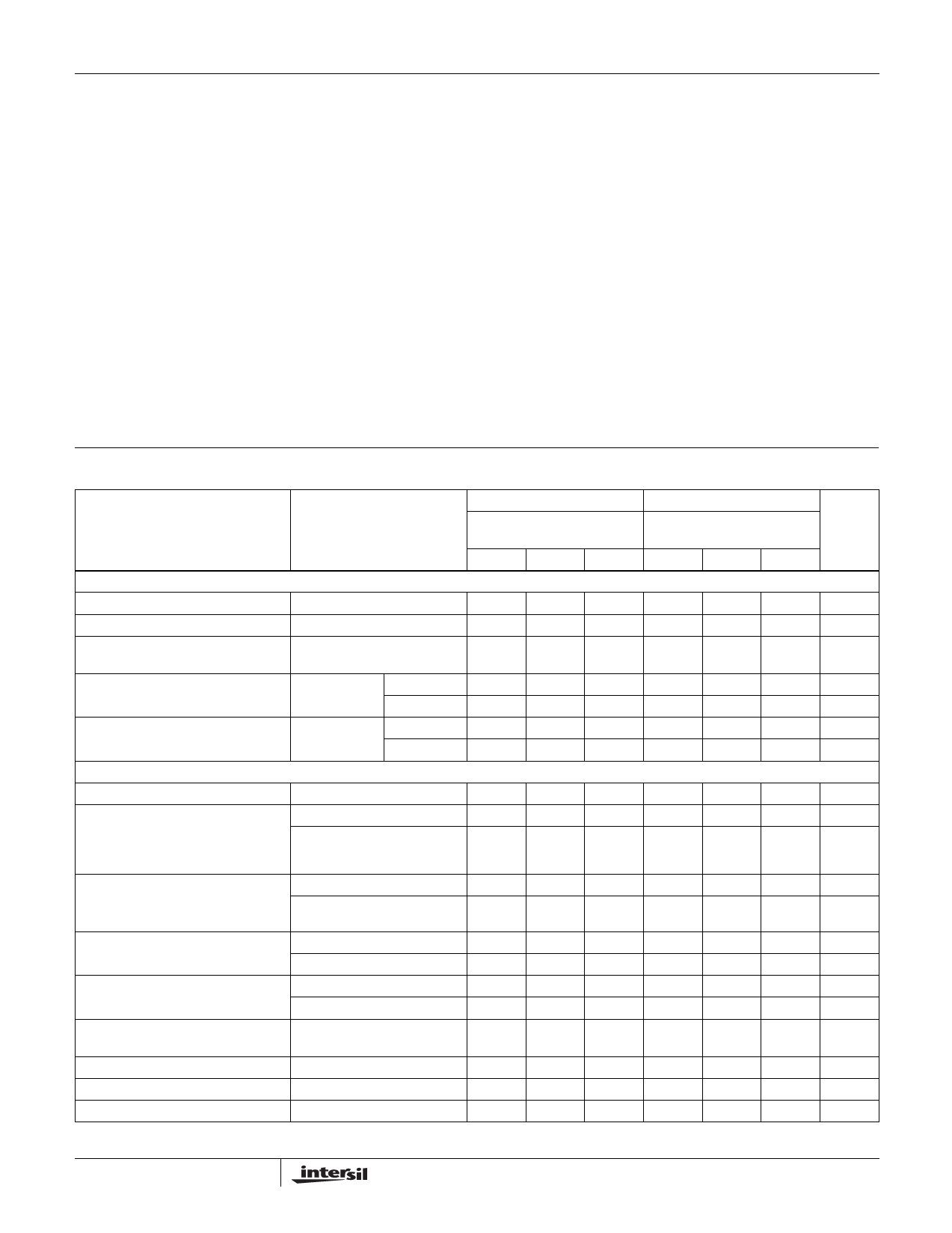
Electrical Specifications AVCC = +5V, DVCC = +5V, AVEE = -5V, DVEE = -5V; Internal Reference Used,
Unless Otherwise Specified
HI5800JCD
0oC TO 70oC
HI5800KCD, HI5800BID
0oC TO 70oC
-40oC TO 85oC
PARAMETER
TEST CONDITIONS
MIN
TYP
MAX
MIN
TYP
MAX
SYSTEM PERFORMANCE
Resolution
12
-
-
12
-
-
Integral Linearity Error, INL
fS = 3MHz, fIN = 45Hz Ramp
-
0.7
±2
Differential Linearity Error, DNL
fS = 3MHz, fIN = 45Hz Ramp
-
±0.5
±1
(Guaranteed No Missing Codes)
-
±0.5
±1
-
±0.3
±1
Offset Error, VOS
(Adjustable to Zero)
(Note 8)
JCD, KCD
-
±2
±15
-
±2
±15
BID
-
-
-
-
±3
±15
Full Scale Error, FSE
(Adjustable to Zero)
(Note 8)
JCD, KCD
-
±2
±15
-
±2
±10
BID
-
-
-
-
±3
±15
DYNAMIC CHARACTERISTICS (Input Signal Level 0.5dB Below Full Scale)
Throughput Rate
No Missing Codes
3.0
-
-
3.0
-
-
Signal to Noise Ratio (SNR)
= R-R----M-M----S-S-----SN----i-og---in-s---ae---l
fS = 3MHz, fIN = 20kHz
fS = 3MHz, fIN = 1MHz
66
69
-
68
71
-
65
67
-
67
69
-
UNITS
Bits
LSB
LSB
LSB
LSB
LSB
LSB
MSPS
dB
dB
Signal to Noise Ratio (SINAD)
= R-----M-----S------NR----oM---i--sS---e---S--+--i-g--D--n--i-as---lt--o---r--t--i-o----n-
Total Harmonic Distortion, THD
Spurious Free Dynamic Range,
SFDR
Intermodulation Distortion, IMD
Differential Gain
Differential Phase
Aperture Delay, tAD
fS = 3MHz, fIN = 20kHz
fS = 3MHz, fIN = 1MHz
fS = 3MHz, fIN = 20kHz
fS = 3MHz, fIN = 1MHz
fS = 3MHz, fIN = 20kHz
fS = 3MHz, fIN = 1MHz
fS = 3MHz, f1 = 49kHz,
f2 = 50kHz (Note 3)
fS = 1MHz
fS = 1MHz
(Note 3)
66
68
-
65
67
-
-
-74
-70
-
-70
-68
71
76
-
68
72
-
-
-74
-66
-
0.9
-
-
0.05
-
-
12
20
68
71
-
dB
67
68
-
dB
-
-85
-74
dBc
-
-77
-70
dBc
76
86
-
dBc
71
77
-
dBc
-
-79
-70
dBc
-
0.9
-
%
-
0.05
-
Degrees
-
12
20
ns
3
Share Link: 