HI5800(1999) Просмотр технического описания (PDF) - Intersil
Номер в каталоге
Компоненты Описание
производитель
HI5800 Datasheet PDF : 15 Pages
| |||
HI5800
interfaced to any type of op amp without a requirement for a
high drive capability. Adequate precautions should be taken
while driving the input from high voltage output op amps to
ensure that the analog input pin is not overdriven above the
specified maximum limits. For a +2.5V reference, the analog
input range is ±2.5V. This input range scales with the value
of the external reference voltage if the internal reference is
not used. For best performance, the analog ground pin next
to the analog input should be utilized for signal return.
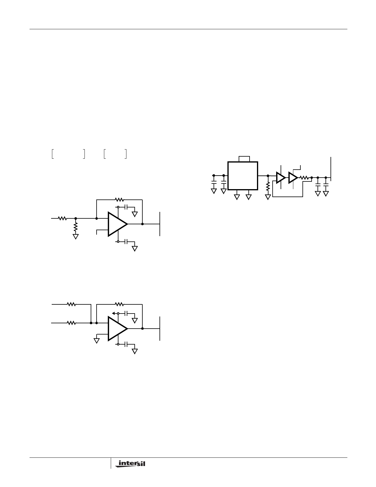
Figures 16 and 17 illustrate the use of an input buffer as a
level shifter to convert a unipolar signal to the bipolar input
used by the HI5800. Figure 16 is an example of a non-
inverting buffer that takes a 0 to 2.5V input and shifts it to
±2.5V. The gain can be calculated from:
VOUT = 1 + (---R-----1-R---|-|-2-R-----3----) × VIN – R-----1---R--+---1--R-----3-- × VOFFSET
R1||R3 = R---R--1---1--+--R---R--3---3--
R2
1kΩ
VOFFSET
R3
2kΩ
+15V
-
R1
2kΩ
+
VIN -15V
0.1
HA2841
VOUT
HI5800
VIN
0.1
FIGURE 16. NON-INVERTING BUFFER
Figure 17 is an example of an inverting buffer that level shifts
a 0V to 5V input to ±2.5V. Its gain can be calculated from:
VOUT = (–R2 ⁄ R1) × VIN – (R2 ⁄ R3) × VOFFSET.
VIN
VOFFSET
R1
1kΩ
R3
2kΩ
R2
1kΩ
+15V
-
0.1
+
HA2841
VOUT
HI5800
VIN
-15V
0.1
FIGURE 17. INVERTING BUFFER
Note that the correct op amp must be chosen in order to not
degrade the overall dynamic performance of the circuit.
Recommended op amps are called out in the figures.
Voltage Reference, REFOUT
The HI5800 has a curvature corrected internal band-gap
reference generator with a buffer amplifier capable of driving up
to 15mA. The band-gap and amplifier are trimmed to give
+2.50V. When connected to the reference input pin REFIN, the
reference is capable of driving up to 2mA externally. Further
loading may degrade the performance of the output voltage. It
is recommended that the output of the reference be decoupled
with good quality capacitors to reduce the high frequency noise.
Reference Input, REFIN
The converter requires a voltage reference connected to the
REFIN pin. This can be the above internal reference or it can
be an external reference. It is recommended that adequate
high frequency decoupling is provided at the reference input
pin in order to minimize overall converter noise.
A user trying to provide an external reference to a HI5800 is
faced with two problems. First, the drift of the reference over
temperature must be very low. Second, it must be capable of
driving the 200Ω input impedance seen at the REFIN pin of
the HI5800. Figure 18 is a recommended circuit for doing
this that is capable of 2ppm/oC drift over temperature.
+15V
+
10µ
0.1
VOUT VFB
REF101
RA
C
RB
10
kΩ
HA5177 HA5002
+15
+15
+
-
-15
10Ω
+
10µ
-15
LOW TC RESISTOR
FIGURE 18. EXTERNAL REFERENCE
HI5800
REFIN
0.1
Supply and Ground Considerations
The HI5800 has separate analog and digital supply and
ground pins to help keep digital noise out of the analog signal
path. For the best performance, the part should be mounted
on a board that provides separate low impedance planes for
the analog and digital supplies and grounds. Only connect the
two grounds together at one place preferably as close as
possible to the part. The supplies should be driven by clean
linear regulated supplies. The board should also have good
high frequency decoupling capacitors mounted as close as
possible to the HI5800.
If the part is powered off a single supply then the analog
supply and ground pins should be isolated by ferrite beads
from the digital supply and ground pins.
Also, it is recommended that the turn-on power supply
sequencing be such that the analog positive supply, AICC,
come up first, followed by the remaining supplies.
Refer to the Application Note “Using Intersil High Speed A/D
Converters” (AN9214) for additional suggestions to consider
when using the HI5800.
Error Adjustments
For most applications the accuracy of the HI5800 is sufficient
without any adjustments. In applications where accuracy is of
utmost importance three external adjustments are possible:
S/H offset, D/A offset and D/A gain. Figure 19 illustrates the use
of external potentiometers to reduce the HI5800 errors to zero.
The D/A offset (ROADJ) and S/H offset (ADJ+ and ADJ-)
trims adjust the voltage offset of the transfer curve while the
11
Share Link: 