HI5800(1999) Просмотр технического описания (PDF) - Intersil
Номер в каталоге
Компоненты Описание
производитель
HI5800 Datasheet PDF : 15 Pages
| |||
HI5800
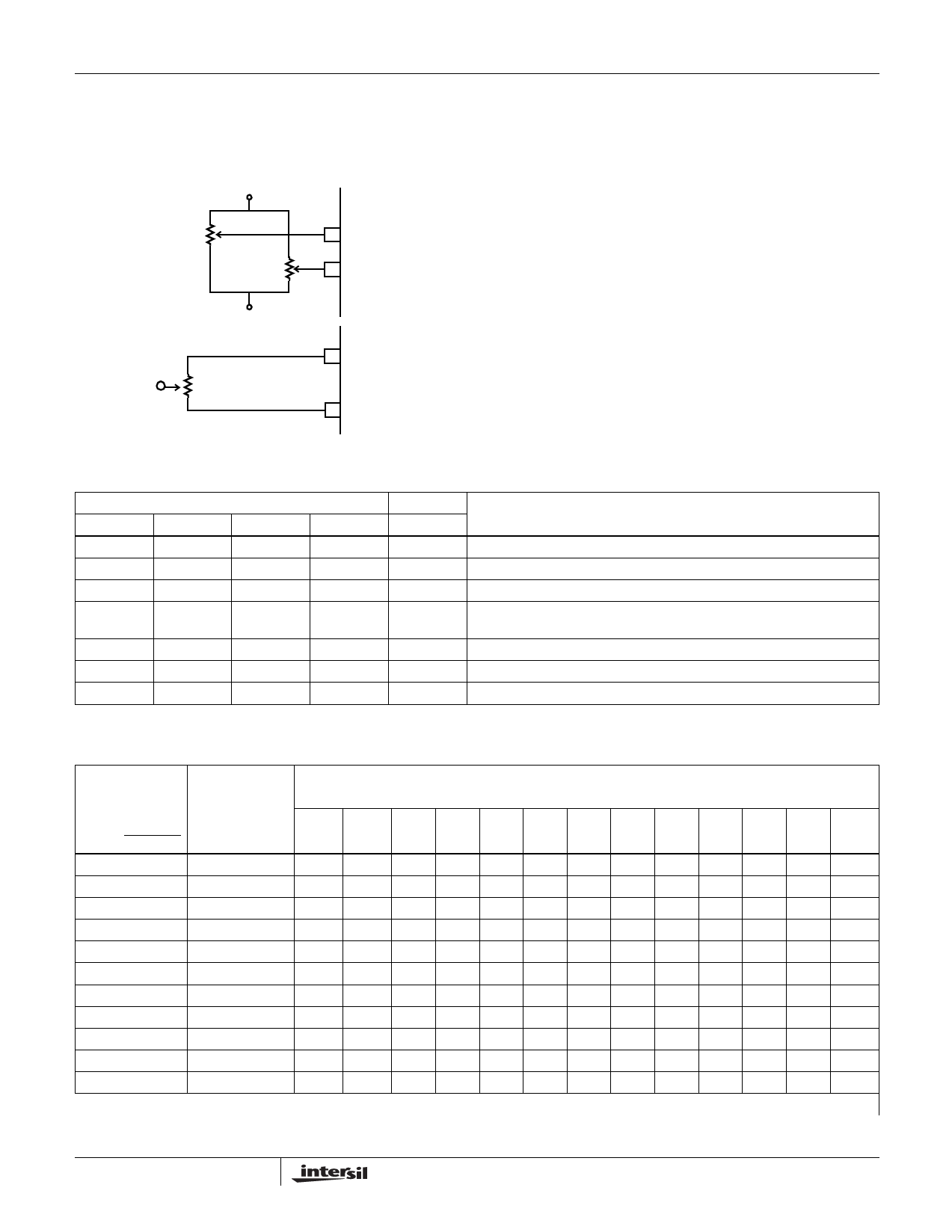
D/A gain trim (RGADJ) adjusts the tilt of the transfer curve
around the curve midpoint (code 2048). The 10kΩ
potentiometers can be installed to achieve the desired
adjustment in the following manner.
VCC
10kΩ
10kΩ
ROADJ
RGADJ
VEE
10kΩ
VEE
ADJ+
ADJ-
Typically only one of the offset trimpots needs to be used.
The offset should first be adjusted to get code 2048 centered
at a desired DC input voltage such as 0V. Next the gain trim
can be adjusted by trimming the gain pot until the 4094 to
4095 code transition occurs at the desired voltage
(2.500V - 1.5 LSBs for a 2.5V reference). The gain trim can
also be done by adjusting the gain pot until the code 0 to 1
transition occurs at a particular voltage (-2.5V + 0.5 LSBs for
a 2.5V reference). If a nonzero offset is needed, then the
offset pot can be adjusted after the gain trim is finished. The
gain trim is simplified if an offset trim to zero is done first with
a nonzero offset trim done after the gain trim is finished. The
D/A offset and S/H offset trimpots have an identical effect on
the converter except that the S/H offset is a finer resolution
trim. The D/A offset and D/A gain typically have an
adjustment range of ±30 LSBs and the S/H offset typically
has an adjustment range of ±20 LSBs.
FIGURE 19. D/A OFFSET, D/A GAIN AND S/H OFFSET
ADJUSTMENTS
TABLE 1. I/O TRUTH TABLE
INPUTS
OUTPUT
CS
CONV
OE
A0
IRQ
FUNCTION
1
X
X
X
X
No operation.
0
0
X
X
X
Continuous convert mode.
0
X
0
0
X
Outputs all 12-bits and OVF or upper byte D11 - D4 in 8 bit mode.
0
X
0
1
X
In 8-bit mode, outputs lower LSBs D3 - D0 followed by 4 trailing zeroes
and OVF (See text).
0
1
X
X
0
Converter is in acquisition mode.
0
X
X
X
1
Converter is busy doing a conversion.
0
X
1
X
X
Data outputs and OVF in high impedance state.
X’s = Don’t Care
TABLE 2. A/D OUTPUT CODE TABLE
CODE
DESCRIPTION
(NOTE)
INPUT
MSB
OUTPUT DATA (OFFSET BINARY)
LSB
VOLTAGE
LSB = 2 (REFIN) REFIN = 2.5V
4096
(V)
OVF D11 D10 D9 D8 D7 D6 D5 D4 D3 D2 D1 D0
≥+FS (Full Scale)
≥ +2.5000
1
1
1
1
1
1
1
1
1
1
1
1
1
+FS - 1 LSB
+3/4 FS
+1/2 FS
+1 LSB
+2.49878
+1.8750
+1.2500
+0.00122
0
1
1
1
1
1
1
1
1
1
1
1
1
0
1
1
1
0
0
0
0
0
0
0
0
0
0
1
1
0
0
0
0
0
0
0
0
0
0
0
1
0
0
0
0
0
0
0
0
0
0
1
0
0.0000
0
1
0
0
0
0
0
0
0
0
0
0
0
-1 LSB
-1/2 FS
-3/4 FS
-FS + 1 LSB
-0.00122
-1.2500
-1.8750
-2.49878
0
0
1
1
1
1
1
1
1
1
1
1
1
0
0
1
0
0
0
0
0
0
0
0
0
0
0
0
0
1
0
0
0
0
0
0
0
0
0
0
0
0
0
0
0
0
0
0
0
0
0
1
≤-FS
≤ -2.5000
1
0
0
0
0
0
0
0
0
0
0
0
0
NOTE: The voltages listed above represent the ideal center of each output code shown as a function of the reference voltage.
12
Share Link: 