MT89L86 Просмотр технического описания (PDF) - Mitel Networks
Номер в каталоге
Компоненты Описание
производитель
MT89L86 Datasheet PDF : 40 Pages
| |||
Advance Information
MT89L86
six address input lines (A0-A5) and four control lines
(CS , DS, R/W and DTA). See Figures 25 to 27 for
each CPU interface timing.
during system power-up to establish the desired
switching configuration as explained in the Serial
Interface and Switching Configurations sections.
The parallel microprocessor port provides the access
to the IMS, Control registers, the Connection
Memory High, the Connection Memory Low and the
Data Memory. All locations can be read or written
except for the data memory which can be read only.
Software Control
The Control register is dynamically used by the CPU
to control switching operations in the MT89L86. The
Control register selects the device's internal
memories and its subsections to specify the input
and output channels selected for switching
procedures.
The address bus on the microprocessor interface
selects the internal registers and memories of the
MT89L86. If the A5 address input is LOW, the
Internal Control, Interface Mode, Stream Pair
Selection and Frame Input Offset registers are
addressed by the A4 to A0 bits according to Table 5.
If the A5 input is HIGH, the remaining address input
lines are used to select memory subsections of up to
128 locations corresponding to the maximum
number of channels per input or output stream. The
address input lines and the Stream Address bits
(STA) of the Control register give the user the
capability of accessing all sections of the MT89L86’s
Data and Connect memories.
The Control and Interface Mode Selection registers
together control all the major functions of the device.
The Interface Mode Select register should be set up
The data in the Control register consists of Split
memory and Message mode bits, Memory select and
Stream Address bits. The memory select bits allow
the Connect Memory HIGH or LOW or the Data
Memory to be chosen, and the Stream Address bits
define an internal memory subsections
corresponding to input or output ST-BUS streams.
Bit 7 (Slip Memory) of the Control register allows
split memory operation whereby reads are from the
Data memory and writes are to the Connect Memory
LOW.
The Message Enable bit (bit 6) places every output
channel on every output stream in message mode;
i.e., the contents of the Connect Memory LOW
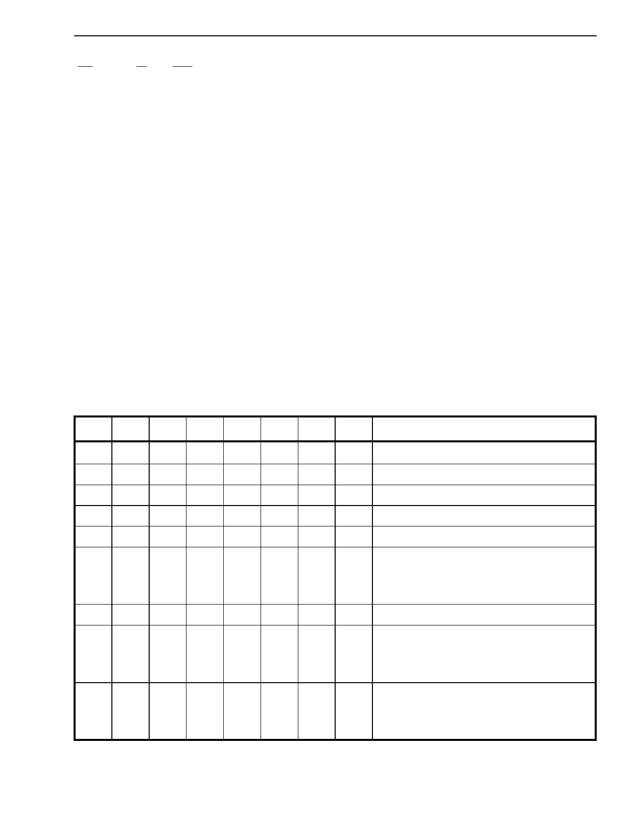
A7 A6 A5 A4 A3 A2 A1 A0
Location
X
X
0
0
0
0
0
0
Control Register
X
X
0
0
0
0
0
1
Interface Mode Select Register
X
X
0
0
0
0
1
0
Stream Pair Select Register
X
X
0
0
0
0
1
1
Frame Input Offset Register
0
0
1
0
0
0
0
0
Channel 0*
0
0
1
0
0
0
0
1
•
•
1
•
•
•
•
•
•
•
1
•
•
•
•
•
0
0
1
1
1
1
1
1
Channel 1*
•
•
Channel 31*
0
1
1
0
0
0
0
0
Channel 32**
0
1
1
0
0
0
0
1
•
•
1
•
•
•
•
•
•
•
1
•
•
•
•
•
0
1
1
1
1
1
1
1
Channel 33**
•
•
Channel 63**
1
0
1
0
0
0
0
0
•
•
1
•
•
•
•
•
•
•
1
•
•
•
•
•
1
1
1
1
1
1
1
1
Channel 64***
•
•
Channel 127***
Table 5 - Address Memory Map
*: channels 0 to 31 are used in 2.048 Mb/s (8 x 8, 16 x 8 and 10 x 10)
**: channels 0 to 63 are used in 4.096 Mb/s (Nibble Switching, 4 x 4, 8 x 4 or Different I/O rates)
***: channels 0 to 127 are used in 8.192 Mb/s (2 x 2 or Different I/O rates)
11
Share Link: 