STB70NF02L Просмотр технического описания (PDF) - STMicroelectronics
Номер в каталоге
Компоненты Описание
производитель
STB70NF02L
STMicroelectronics

STB70NF02L Datasheet PDF : 7 Pages
| |||
STB70NF02L
N-CHANNEL 20V - 0.006 Ω - 70A D2PAK
LOW GATE CHARGE STripFET™II POWER MOSFET
PRELIMINARY DATA
TYPE
VDSS
RDS(on)
ID
STB70NF02L
20 V <0.009Ω 70 A
s TYPICAL RDS(on) = 0.016 Ω
s TYPICAL Qg = 36 nC @ 10 V
s OPTIMAL RDS(on) x Qg TRADE-OFF
s CONDUCTION LOSSES REDUCED
s SWITCHING LOSSES REDUCED
DESCRIPTION
This application specific Power MOSFET is the third
genaration of STMicroelectronis unique "Single Feature
Size™" strip-based process. The resulting transistor
shows the best trade-off between on-resistance and gate
charge. When used as high and low side in buck
regulators, it gives the best performance in terms of both
conduction and switching losses. This is extremely
important for motherboards where fast switching and
high efficiency are of paramount importance.
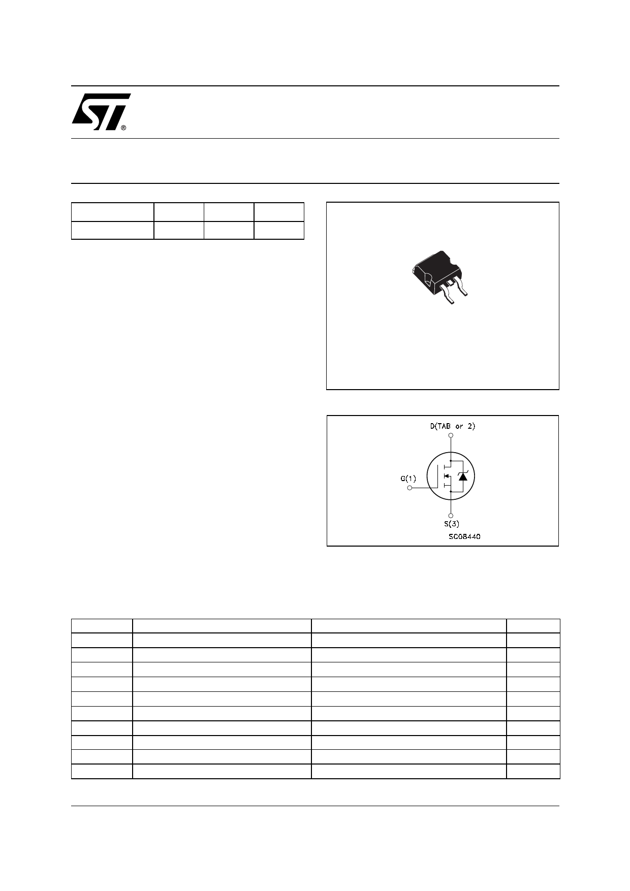
3
1
D2PAK
TO-263
(Suffix “T4”)
ADD SUFFIX “T4” FOR ORDERING IN TAPE & REEL
INTERNAL SCHEMATIC DIAGRAM
APPLICATIONS
s SPECIFICALLY DESIGNED AND OPTIMISED
FOR HIGH EFFICIENCY CPU CORE DC/DC
CONVERTERS
ABSOLUTE MAXIMUM RATINGS
Symbol
Parameter
VDS
Drain-source Voltage (VGS = 0)
VDGR
Drain-gate Voltage (RGS = 20 kΩ)
VGS
Gate- source Voltage
ID
Drain Current (continuous) at TC = 25°C
ID
Drain Current (continuous) at TC = 100°C
IDM(•)
Drain Current (pulsed)
Ptot
Total Dissipation at TC = 25°C
Derating Factor
Tstg
Storage Temperature
Tj
Max. Operating Junction Temperature
(•) Pulse width limited by safe operating area
Value
20
20
± 18
70
50
280
100
0.67
-65 to 175
175
Unit
V
V
V
A
A
A
W
W/°C
°C
°C
March 2002
1/7
This is preliminary information on a new product now in development or undergoing evaluation. Details are subject to change without notice.
Share Link: