TDA9812 Просмотр технического описания (PDF) - Philips Electronics
Номер в каталоге
Компоненты Описание
производитель
TDA9812 Datasheet PDF : 32 Pages
| |||
Philips Semiconductors
Multistandard VIF-PLL and
FM-PLL/AM demodulator
Preliminary specification
TDA9812
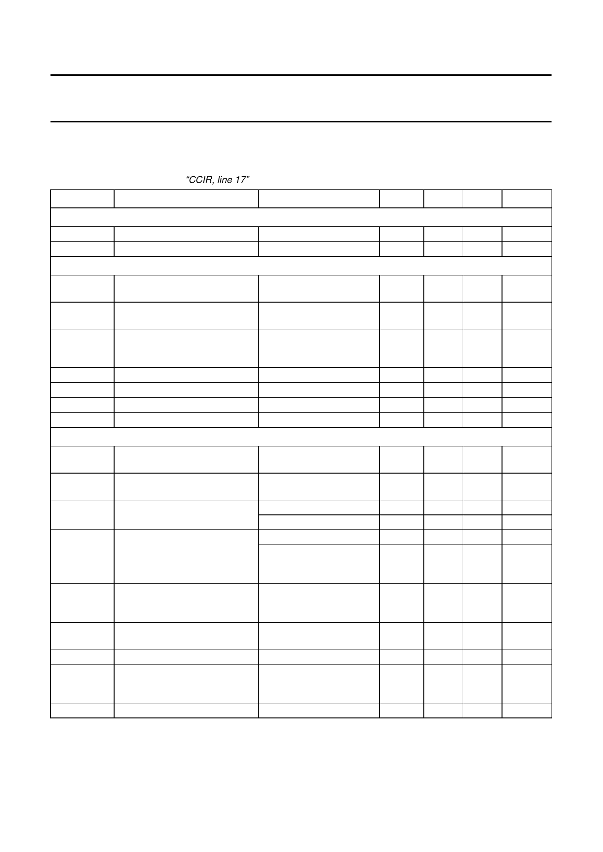
CHARACTERISTICS
SDIP32 pinning; VP = 5 V; Tamb = +25 °C; see Table 1 for input frequencies and level; input level Vi IF 1, 2 = 10 mV
RMS value (sync-level for B/G, peak white level for L); video modulation DSB; residual carrier B/G: 10%; L = 3%;
video signal in accordance with “CCIR, line 17”; measurements taken in Fig.17 unless otherwise specified.
SYMBOL
PARAMETER
CONDITIONS
MIN. TYP. MAX. UNIT
Supply (pin 29)
VP
supply voltage
note 1
4.5
IP
supply current
82
Vision IF amplifier (pins 1 and 2)
Vi(VIF)(rms)
input signal voltage sensitivity
(RMS value)
B/G standard; −1 dB video −
at output
Vi(max)(rms) maximum input signal voltage B/G standard; +1 dB
120
(RMS value)
video at output
∆Vo(int)
internal IF amplitude difference within AGC range;
−
between picture and sound
B/G standard;
carrier
∆f = 5.5 MHz
GIF
IF gain control range
see Figs 5 and 6
65
Ri(diff)
differential input resistance
note 2
1.7
Ci(diff)
differential input capacitance note 2
1.2
V1/2
DC input voltage
−
True synchronous video demodulator; see note 3
fVCO(max)
maximum oscillator frequency f = 2fpc
125
for carrier regeneration
∆fVCO
oscillator drift (free-running) as a IAFC = 0; note 4
−20
function of temperature
V0 ref(rms)
oscillator voltage swing at
B/G and L standard
70
pins 24 and 25 (RMS value)
L/L accent standard
45
∆fpc(capt)
∆fpc(ff)
∆fpc(alg)
vision carrier capture frequency
range
vision carrier frequency
(free-running) accuracy
L/L accent alignment frequency
range
B/G and L standard
L/L accent standard;
fpc = 33.9 MHz;
R11 = 5.6 kΩ
L/L accent standard;
fpc = 33.9 MHz;
R11 = 5.6 kΩ
IAFC = 0
±1.5
±1.0
−
±400
tacqu
Vi (VIF)(rms)
acquisition time
BL = 60 kHz; note 5
−
VIF input signal voltage
maximum IF gain; note 6 −
sensitivity for PLL to be locked
(RMS value; pins 1 and 2)
IPLL(os)
FPLL offset current at pin 7
note 7
−
5
5.5
V
96
110 mA
60
100 µV
200 −
mV
0.7
1
dB
70
−
dB
2.2
2.7
kΩ
1.7
2.5
pF
3.4
−
V
130 −
−
+20
100 130
65
85
±2.0 −
±1.3 −
MHz
ppm/K
mV
mV
MHz
MHz
±200 ±400 kHz
±600 −
kHz
−
30
ms
30
70
µV
−
±4.5 µA
1995 Mar 21
10
Share Link: 