PBL40305 Просмотр технического описания (PDF) - Ericsson
Номер в каталоге
Компоненты Описание
производитель
PBL40305 Datasheet PDF : 7 Pages
| |||
PBL 403 05
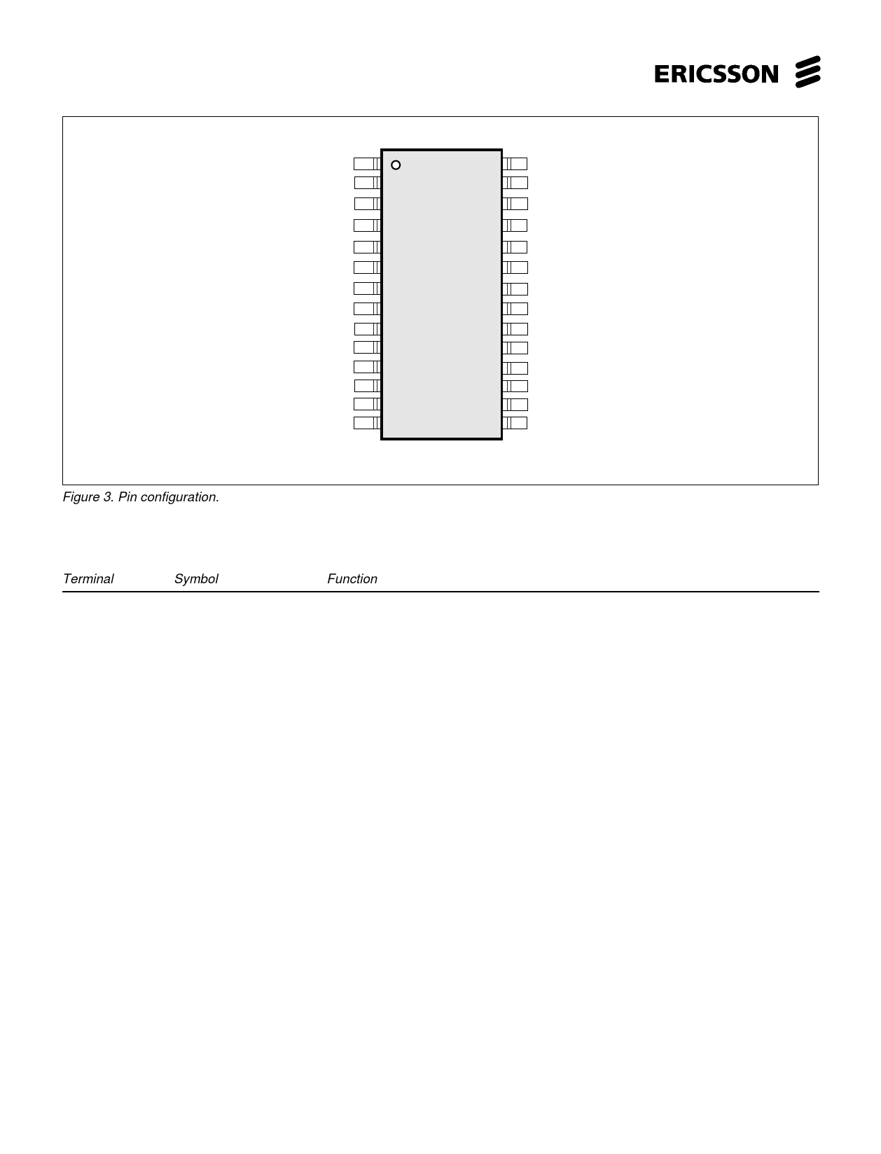
Figure 3. Pin configuration.
CA 1
VNEG 2
VSEL 3
VAPC 4
VD1_DCS 5
GND 6
RFIN_DCS 7
GND 8
RFIN_GSM 9
GND 10
VD1_GSM 11
GND 12
VD3_GSM1 13
VD3_GSM2 14
28 VDC
27 GND
26 VD3_DCS2
25 VD3_DCS1
24 GND
23 GND
22 VD2_DCS
21 GND
20 VD2_GSM
19 GND
18 GND
17 RFOUT_GSM2
16 RFOUT_GSM1
15 GND
Terminal
1
2
3
4
5
6,8,10,12,15,
18,19,21,23,
24,27
7
9
11
13, 14
16,17
20
22
25,26
28
Symbol
CA
VNEG
VSEL
VAPC
VD1_DCS
GND
RFIN_DCS
RFIN_GSM
VD1_GSM
VD3_GSM
RFOUT_GSM
VD2_GSM
VD2_DCS
VD3_DCS
VDC
Function
Separate Current Source +terminal
Negative supply
Digital band select function
Analog output power control
Power supply for 1st stage of high band chain
AC coupled 50ohm input
AC coupled 50ohm input
Power supply for 1st stage of low band chain
Power supply for output stage stage of low band chain
Power supply for 2nd stage of low band chain
Power supply for 2nd stage of high band chain
RF output and power supply for output stage of high band chain
Separate Current Source -terminal
4
Share Link: 