NTE2900 Просмотр технического описания (PDF) - NTE Electronics
Номер в каталоге
Компоненты Описание
производитель
NTE2900 Datasheet PDF : 3 Pages
| |||
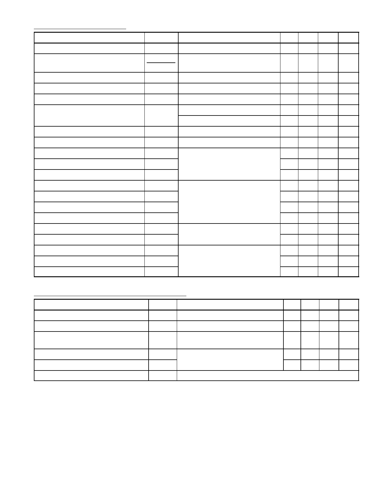
Electrical Characteristics: (TJ = +25°C unless otherwise specified)
Parameter
Symbol
Test Conditions
Min Typ Max Unit
Drain–to–Source Breakdown Voltage V(BR)DSS VGS = 0V, ID = 250µA
250 –
–
V
Breakdown Voltage Temp. Coefficient
Static Drain–to–Source On–Resistance
∆V(BR)DSS
∆TJ
RDS(on)
Reference to +25°C, ID = 1mA
VGS = 10V, ID = 8.4A, Note 4
– 0.34 – V/°C
– – 0.28 Ω
Gate Threshold Voltage
VGS(th) VDS = VGS, ID = 250µA
2.0 – 4.0 V
Forward Transconductance
gfs
VDS = 50V, ID = 8.4A, Note4
6.7 –
– mhos
Drain–to–Source Leakage Current
IDSS VDS = 250V, VGS = 0V
– – 25 µA
VDS = 200V, VGS = 0V, TJ = +125°C –
– 250 µA
Gate–to–Source Forward Leakage
IGSS VGS = 20V
– – 100 nA
Gate–to–Source Reverse Leakage
IGSS VGS = –20V
– – –100 nA
Total Gate Charge
Gate–to–Source Charge
Qg
ID = 7.9A, VDS = 200V, VGS = 10V, –
–
68 nC
Qgs
Note 4
– – 11 nC
Gate–to–Drain (“Miller”) Charge
Qgd
– – 35 nC
Turn–On Delay Time
Rise Time
td(on) VDD = 125V, ID = 7.9A, RG = 9.1Ω, –
11
–
ns
tr
RD = 8.7Ω, Note 4
– 24 – ns
Turn–Off Delay Time
td(off)
– 53 – ns
Fall Time
tf
– 49 – ns
Internal Drain Inductance
Internal Source Inductance
LD
Between lead, .250in. (6.0) mm from – 4.5 – nH
LS
package and center of die contact
– 7.5 – nH
Input Capacitance
Ciss
VGS = 0V, VDS = 25V, f = 1MHz
– 1300 – pF
Output Capacitance
Coss
– 330 – pF
Reverse Transfer Capaticance
Crss
– 85 – pF
Source–Drain Ratings and Characteristics:
Parameter
Symbol
Test Conditions
Min Typ Max Unit
Continuous Source Current (Body Diode)
Pulsed Source Current (Body Diode)
Diode Forward Voltage
IS
ISM Note 1
VSD TJ = +25°C, IS = 14A, VGS = 0V,
Note 4
– – 14 A
– – 56 A
– – 1.8 V
Reverse Recovery Time
Reverse Recovery Charge
trr TJ = +25°C, IF = 7.9A,
Qrr di/dt = 100A/µs, Note 4
– 250 500 ns
– 2.3 4.6 µC
Forward Turn–On Time
ton Intrinsic turn–on time is neglegible (turn–on is dominated by LS+LD)
Note 1. Repetitive rating; pulse width limited by maximum junction temperature.
Note 4. Pulse width ≤ 300µs; duty cycle ≤ 2%.
Share Link: 