TQ1089-MC500 Просмотр технического описания (PDF) - TriQuint Semiconductor
Номер в каталоге
Компоненты Описание
производитель
TQ1089-MC500 Datasheet PDF : 10 Pages
| |||

TQ1089
Layout Guidelines
Multiple ground and power pins on the TQ1089 reduce
ground bounce. Good layout techniques, however, are
necessary to guarantee proper operation and to meet
the specifications across the full operating range.
TriQuint recommends bypassing each of the VDD supply
pins to the nearest ground pin, as close to the chip
as possible.
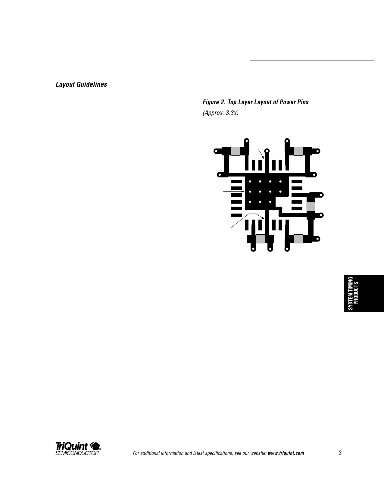
Figure 2. Top Layer Layout of Power Pins
(Approx. 3.3x)
VDD
C4
Pin 1
VDD
C3
Figure 2 shows the recommended power layout for the
TQ1089. The bypass capacitors should be located on
the same side of the board as the TQ1089. The VDD
traces connect to an inner-layer VDD plane. All of the
ground pins (GND) are connected to a small ground
plane on the surface beneath the chip. Multiple through
holes connect this small surface plane to an inner-layer
ground plane. The capacitors (C1–C5) are 0.1 mF.
TriQuint’s test board uses X7R temperature-stable
capacitors in 1206 SMD cases.
Ground
Plane
Pin 15
C5
VDD
VDD
C2
C1
VDD
For additional information and latest specifications, see our website: www.triquint.com
3