GA1087 Просмотр технического описания (PDF) - TriQuint Semiconductor
Номер в каталоге
Компоненты Описание
производитель
GA1087 Datasheet PDF : 10 Pages
| |||
GA1087
Functional Description
The core of the GA1087 is a Phase-Locked Loop (PLL)
that continuously compares the reference clock (REFCLK)
to the feedback clock (FBIN), maintaining a zero frequency
difference between the two. Since one of the outputs
(Q0–Q8) is always connected to FBIN, the PLL keeps
the propagation delay between the outputs and the
reference clock within –350 ps +500 ps for the
GA1087-MC500, and within –350 ps +700 ps for the
GA1087-MC700.
The internal voltage-controlled oscillator (VCO) has an
operating range of 280 MHz to 420 MHz. The combi-
nation of the VCO and the Divide Logic enables the
GA1087 to operate between 24 MHz and 105 MHz.
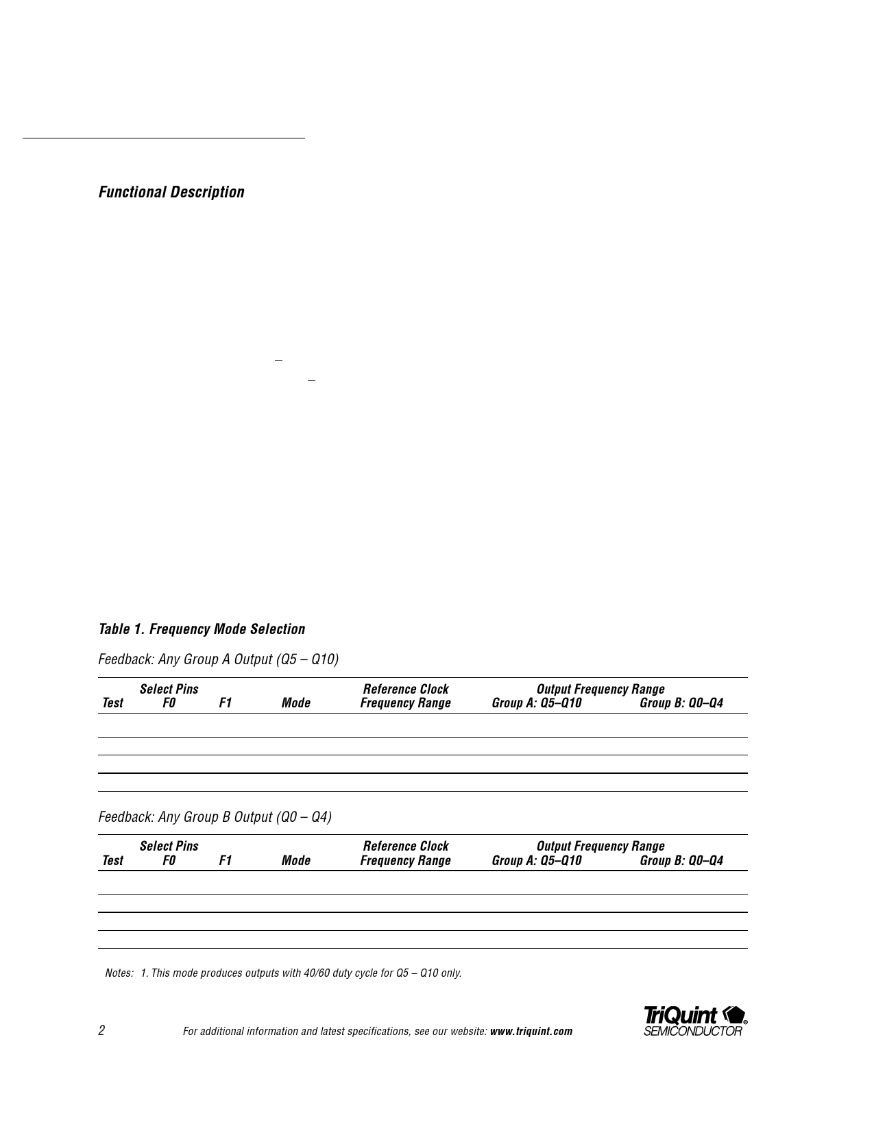
The device features six divide modes: ÷4, ÷5, ÷6, ÷8,
÷10, and ÷12. The Frequency Select pins, F0 and F1,
and the output used as feedback to FBIN set the divide
mode as shown in Table 1.
In the test mode, the PLL is bypassed and REFCLK is
connected directly to the Divide Logic block via the
MUX, as shown in Figure 1. This mode is useful for
debug and test purposes. The various test modes are
outlined in Table 2. In the test mode, the frequency of
the reference clock is divided by 4, 5, or 6.
The maximum rise and fall time at the output pins is
1.4 ns. All outputs of the GA1087 are TTL-compatible
with 30 mA symmetric drive and a minimum VOH of 2.4 V.
Power Up/Reset Synchronization
After-power-up or reset, the PLL requires time before it
achieves synchronization lock. The maximum time
required for synchronization (TSYNC) is 500 ms.
Table 1. Frequency Mode Selection
Feedback: Any Group A Output (Q5 – Q10)
Select Pins
Test
F0
F1
0
1
0
0
0
0
0
0
1
0
1
1
Mode
÷4
÷5
÷6
Not Used
Reference Clock
Frequency Range
70 MHz – 105 MHz
56 MHz – 84 MHz
48 MHz – 70 MHz
N.A.
Feedback: Any Group B Output (Q0 – Q4)
Select Pins
Test
F0
F1
0
1
0
0
0
0
0
0
1
0
1
1
Mode
÷8
÷ 10
÷ 12
Not Used
Reference Clock
Frequency Range
35 MHz – 52 MHz
28 MHz – 42 MHz
24 MHz – 35 MHz
N.A.
Notes: 1. This mode produces outputs with 40/60 duty cycle for Q5 – Q10 only.
Output Frequency Range
Group A: Q5–Q10
Group B: Q0–Q4
70 MHz – 105 MHz
56 MHz – 84 MHz 1
48 MHz – 70 MHz
N.A.
35 MHz – 52 MHz
28 MHz – 42 MHz
24 MHz – 35 MHz
N.A.
Output Frequency Range
Group A: Q5–Q10
Group B: Q0–Q4
70 MHz – 105 MHz
56 MHz – 84 MHz 1
48 MHz – 70 MHz
N.A.
35 MHz – 52 MHz
28 MHz – 42 MHz
24 MHz – 35 MHz
N.A.
2
For additional information and latest specifications, see our website: www.triquint.com
Share Link: 