GA1086MC500 Просмотр технического описания (PDF) - TriQuint Semiconductor
Номер в каталоге
Компоненты Описание
производитель
GA1086MC500 Datasheet PDF : 12 Pages
| |||
GA1086
Power-Up/Reset Synchronization
The GA1086 utilizes on-chip phase-locked loop (PLL)
technology to maintain synchronization between inputs
and outputs. Whenever the device is powered up, or
the system clock (CLK) is reset, the phase-locked loop
requires a synchronization time (tSYNC) before lock is
achieved. The maximum time required for
synchronization is 500 ms.
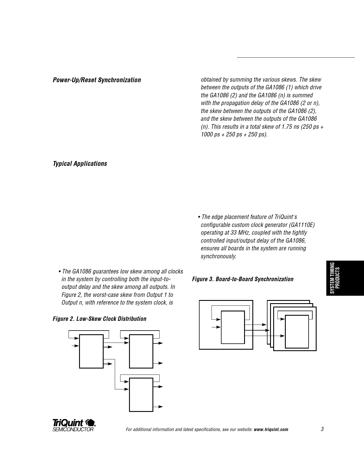
obtained by summing the various skews. The skew
between the outputs of the GA1086 (1) which drive
the GA1086 (2) and the GA1086 (n) is summed
with the propagation delay of the GA1086 (2 or n),
the skew between the outputs of the GA1086 (2),
and the skew between the outputs of the GA1086
(n). This results in a total skew of 1.75 ns (250 ps +
1000 ps + 250 ps + 250 ps).
2) Board-to-Board Synchronization
Typical Applications
The GA1086 is designed to satisfy a wide range of
system clocking requirements. Following are two of the
most common clocking bottlenecks which can be
solved using the GA1086.
Many computing systems today consist of multiple
boards designed to run synchronously. The skew
associated with routing clocks across a backplane
presents a major hurdle to maximizing system
performance.
1) Low-Skew Clock Distribution / Clock Trees
The most basic bottleneck to clocking high-performance
systems is generating multiple copies of a system clock,
while maintaining low skew throughout the system.
• The edge placement feature of TriQuint's
configurable custom clock generator (GA1110E)
operating at 33 MHz, coupled with the tightly
controlled input/output delay of the GA1086,
ensures all boards in the system are running
synchronously.
• The GA1086 guarantees low skew among all clocks
in the system by controlling both the input-to-
output delay and the skew among all outputs. In
Figure 2, the worst-case skew from Output 1 to
Output n, with reference to the system clock, is
Figure 3. Board-to-Board Synchronization
HOST
TARGETS
Figure 2. Low-Skew Clock Distribution
SYSTEM
CLOCK
Q1
GA1086
(1)
•
•
•
Q/2
Q1
GA1086
(2)
Q9
OUTPUT 1
•
•
•
SYS
CLK
GA1110E
t
GA1000
–t
–2t
GA1086
GA1086
(n)
•
•
•
OUTPUT n
For additional information and latest specifications, see our website: www.triquint.com
3
Share Link: 