ADSQ-1410 Просмотр технического описания (PDF) - Murata Power Solutions
Номер в каталоге
Компоненты Описание
производитель
ADSQ-1410 Datasheet PDF : 11 Pages
| |||
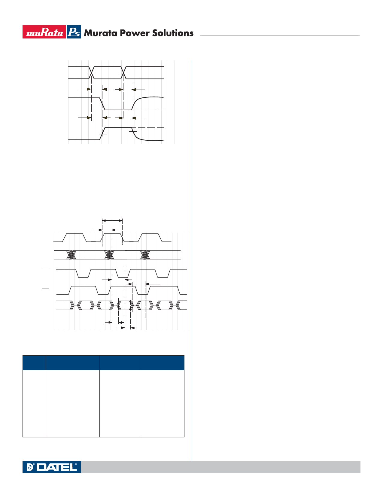
ENABLE
➀ Output tPZL
waveform 1
S1 at VCC
t PZH
➁ Output
waveform 1
S1 at GND
50% VCC
50% VCC
50% VCC
VCC
0V
t PZL
–VCC
VOL +0.3V VOL
VOH +0.3V VOH
50% VCC
–0V
Voltage Waveforms
Enable and Disable Times
Low- and High-Level Enabling
Enable and Disable Times
➀ Waveform 1 is for an output with internal conditions such that the output is active LO and
Hi-Z is pulled 3.3VD through 1k resistor
➁ Waveform 2 is for an output with internal conditions such that the output is active LO and
Hi-Z is pulled GND through 1k resistor
START
CONVERT
18ns typ
N
(tod)
50ns typ.
DATA➀
N-3
N-2
N-1
EN A
EN B
30ns
30ns
DATA
A or B OUT
or
(C or D OUT)
DATA-A
N-3
DATA-B
N-3
DATA-A
N-2
6.6ns
➀ Assuming single channel OUTPUT ENABLED
7.8ns
Enable Timing Diagram
DATA-B
N-2
DATA-A
N-1
Overflow
1
0
0
0
0
0
0
0
0
1
Output Coding
MSB
LSB
11 1111 1111 1111
11 1111 1111 1111
11 1100 0000 0000
11 0000 0000 0000
10 0000 0000 0000
01 0000 0000 0000
00 1000 0000 0000
00 0000 0000 0001
00 0000 0000 0000
00 0000 0000 0000
Input Range
±2.5V
+2.499847
+2.499695
+1.875000
+1.250000
±0.000000
–1.250000
–1.875000
–2.499848
–2.500000
–2.500153
Table 3. Output Coding
Bipolar Scale
+FS – 1/2LSB
+FS – 1LSB
3/4 FS
+1/2 FS
0
–1/2 FS
–3/4 FS
–FS +1LSB
–FS
–FS –1/2LSB
ADSQ-1410
Quad 14-Bit, 10 MSPS Sampling A/D Converter
Start Convert Considerations
The START CONV command of the ADSQ-1410 is buffered internally prior
to being distributed to each A/D convert. The multi-stage architecture of
the internal A/D’s uses both the rising and falling edges of each START
CONV pulse in the conversion process and therefore requires START CONV
commands that maintain a minimum of 45ns for both the high and the low
times. At 10MHz clock rate this would require a 50% (±5% )duty cycle.
Due to the analog pipeline architecture of the A/D section a Start Convert
period that exceeds 1ms will allow internal sample and holds to discharge
the held voltages thereby affecting output integrity. Consequently a mini-
mum Start convert rate of 1 kHz is specified.
Clock jitter (aperture jitter) will result in a variation of time interval
between successive A/D conversions which can adversely affect the signal
to noise ratio performance. Low jitter crystal oscillators provide clock
signals at a 50% duty cycle making ideal START CONV sources. Input logic
levels for EN_ pins are dictated by +VDD supply voltage; logic level for
START_CONV is a function of +5V supply. See Functional Specifications:
Digital Inputs.
Layout Considerations
Although the ADSQ-1410 functions in both the analog and digital realms,
in regards to layout it should be treated as an analog component.
Grounding is critical in any high-speed, high resolution data acquisition
system. As such a multilayer PCB is recommended to allow ground planes
as well as isolation of digital and analog signals. Ground planes will sig-
nificantly reduce impedance and minimize signal return loops. In addition,
the power and ground planes can be arranged so as to provide inherent
distributed capacitance within the PCB.
The AGND, SGND and OGND grounds should all be connected to a
common ground plane directly beneath the ADSQ-1410. Although using a
common plane beneath the A/D, it may be beneficial to design notches or
“keep-outs” in the ground plane so as to steer ground currents away from
critical signal sensitive areas in the ground plane.
Each channel of the quad A/D operates from its own supply voltages.
Bypassing from each of these supplies should be done as close to the
respective power and associated ground pins as possible. Bypass ceramic
capacitor values of 1uF and 0.1uF are recommended in most application.
In order to prevent digital switching noise from being coupled into sensi-
tive analog signal paths, the layout designer should assure that digital
signals do not run parallel with signal traces. For ease of layout the ADSQ-
1410 is designed with all Digital Outputs and START CONVERT one side of
the package and signal pins on the other.
The +2.5V REF pin is used in conjunction with external components to set
the RANGE of each channel. Care should be exercised to assure that the
Reference voltage and its associated divided down voltage applied to the
RANGE pins are bypassed properly and not subject to noise pickup from
digital paths.
Typical Application Connection Diagram
The ADSQ-1410 is a functionally complete quad A/D and as such requires
little externally circuitry for operation. The figure (connection diagram)
shows the typical circuit connections with channels A, B, C operating with
a ±2.5V input range and channel D operating with a gain adjustable input
range less than ±2.5V.
www.murata-ps.com
Technical enquiries email: data.acquisition@murata-ps.com, tel: +1 508 339 3000
MDA_ADSQ.B01 Page 5 of 11
Share Link: 