KF3N40D Просмотр технического описания (PDF) - KEC
Номер в каталоге
Компоненты Описание
производитель
KF3N40D Datasheet PDF : 6 Pages
| |||
KF3N40D/I
ELECTRICAL CHARACTERISTICS (Tc=25℃)
CHARACTERISTIC
SYMBOL
TEST CONDITION
Static
Drain-Source Breakdown Voltage
Breakdown Voltage Temperature Coefficient
Drain Cut-off Current
Gate Threshold Voltage
Gate Leakage Current
Drain-Source ON Resistance
Dynamic
BVDSS
ID=250μA, VGS=0V
ΔBVDSS/ΔTj ID=250μA, Referenced to 25℃
IDSS
VDS=400V, VGS=0V,
Vth
VDS=VGS, ID=250μA
IGSS
VGS=±30V, VDS=0V
RDS(ON)
VGS=10V, ID=1.1A
Total Gate Charge
Gate-Source Charge
Gate-Drain Charge
Qg
Qgs
VDS=320V, ID=2.2A
VGS=10V
(Note4,5)
Qgd
Turn-on Delay time
Turn-on Rise time
Turn-off Delay time
Turn-off Fall time
td(on)
tr
td(off)
tf
VDD=200V, ID=2.2A
RG=25Ω
VGS=10V
(Note4,5)
Input Capacitance
Ciss
Output Capacitance
Coss
VDS=25V, VGS=0V, f=1.0MHz
Reverse Transfer Capacitance
Crss
Source-Drain Diode Ratings
Continuous Source Current
Pulsed Source Current
IS
VGS<Vth
ISP
Diode Forward Voltage
VSD
IS=2.2A, VGS=0V
Reverse Recovery Time
Reverse Recovery Charge
trr
IS=2.2A, VGS=0V,
Qrr
dIs/dt=100A/μs
Note 1) Repetivity rating : Pulse width limited by junction temperature.
Note 2) L = 19mH, IS=2.2A, VDD=50V, RG = 25Ω, Starting Tj = 25℃.
Note 3) IS ≤2A, dI/dt≤200A/㎲, VDD≤BVDSS, Starting Tj = 25℃.
Note 4) Pulse Test : Pulse width ≤ 300㎲, Duty Cycle ≤ 2%.
Note 5) Essentially independent of operating temperature.
MIN. TYP. MAX. UNIT
400
-
-
V
-
0.4
-
V/℃
-
-
10
μA
2.5
-
4.5
V
-
- ±100 nA
-
2.8
3.4
Ω
-
4.4
5.8
-
1.0
-
nC
-
2.0
-
-
10
-
-
11
-
ns
-
20
-
-
17
-
-
163 211
-
26
-
pF
-
2.5
-
-
-
2
A
-
-
8
-
-
1.4
V
-
240
-
ns
-
0.65
-
μC
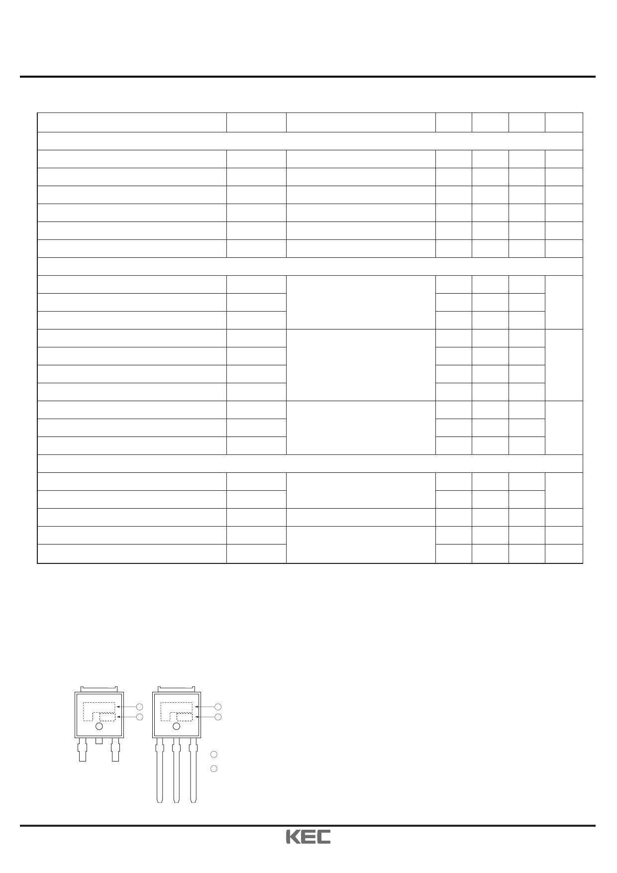
Marking
KF3N40
1
KF3N40
1
D 001
2
I 001
2
1 PRODUCT NAME
2 LOT NO
2010. 8. 23
Revision No : 0
2/6
Share Link: 