MLD1N06CL Просмотр технического описания (PDF) - Motorola => Freescale
Номер в каталоге
Компоненты Описание
производитель
MLD1N06CL
Motorola => Freescale

MLD1N06CL Datasheet PDF : 6 Pages
| |||
MLD1N06CL
ELECTRICAL CHARACTERISTICS (TC = 25°C unless otherwise noted)
Characteristic
Symbol
Min
Typ
Max
Unit
OFF CHARACTERISTICS
Drain–to–Source Breakdown Voltage (Internally Clamped)
(ID = 20 mAdc, VGS = 0 Vdc)
(ID = 20 mAdc, VGS = 0 Vdc, TJ = 150°C)
Zero Gate Voltage Drain Current
(VDS = 45 Vdc, VGS = 0 Vdc)
(VDS = 45 Vdc, VGS = 0 Vdc, TJ = 150°C)
Gate–Source Leakage Current
(VG = 5.0 Vdc, VDS = 0 Vdc)
(VG = 5.0 Vdc, VDS = 0 Vdc, TJ = 150°C)
V(BR)DSS
Vdc
59
62
65
59
62
65
IDSS
—
—
µAdc
0.6
5.0
6.0
20
IGSS
—
—
µAdc
0.5
5.0
1.0
20
ON CHARACTERISTICS(1)
Gate Threshold Voltage
(ID = 250 µAdc, VDS = VGS)
(ID = 250 µAdc, VDS = VGS, TJ = 150°C)
Static Drain–to–Source On–Resistance
(ID = 1.0 Adc, VGS = 4.0 Vdc)
(ID = 1.0 Adc, VGS = 5.0 Vdc)
(ID = 1.0 Adc, VGS = 4.0 Vdc, TJ = 150°C)
(ID = 1.0 Adc, VGS = 5.0 Vdc, TJ = 150°C)
Static Source–to–Drain Diode Voltage (IS = 1.0 Adc, VGS = 0 Vdc)
Static Drain Current Limit
(VGS = 5.0 Vdc, VDS = 10 Vdc)
(VGS = 5.0 Vdc, VDS = 10 Vdc, TJ = 150°C)
Forward Transconductance (ID = 1.0 Adc, VDS = 10 Vdc)
RESISTIVE SWITCHING CHARACTERISTICS(2)
Turn–On Delay Time
Rise Time
Turn–Off Delay Time
(VDD = 25 Vdc, ID = 1.0 Adc,
VGS(on) = 5.0 Vdc, RGS = 50 Ohms)
Fall Time
INTERNAL PACKAGE INDUCTANCE
Internal Drain Inductance
(Measured from drain lead 0.25” from package to center of die)
VGS(th)
1.0
0.6
RDS(on)
—
—
—
—
VSD
—
ID(lim)
2.0
1.1
gFS
1.0
td(on)
—
tr
—
td(off)
—
tf
—
LD
—
Vdc
1.5
2.0
—
1.6
Ohms
0.63
0.75
0.59
0.75
1.1
1.9
1.0
1.8
1.1
1.5
Vdc
Adc
2.3
2.75
1.3
1.8
1.4
—
mhos
1.2
2.0
ns
4.0
6.0
4.0
6.0
3.0
5.0
nH
4.5
—
Internal Source Inductance
LS
nH
(Measured from the source lead 0.25” from package to source bond pad)
—
7.5
—
(1) Pulse Test: Pulse Width ≤ 300 µs, Duty Cycle ≤ 2%.
(2) Switching characteristics are independent of operating junction temperature.
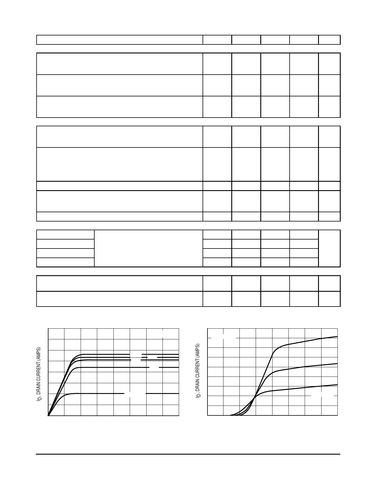
4
TJ = 25°C
4 VDS ≥ 7.5 V
3
10 V
6V
8V
3
4V
2
2
–50°C
25°C
1
VGS = 3 V
1
TJ = 150°C
0
0
2
4
6
8
VDS, DRAIN–TO–SOURCE VOLTAGE (VOLTS)
0
0
2
4
6
8
VGS, GATE–TO–SOURCE VOLTAGE (VOLTS)
Figure 1. Output Characteristics
Figure 2. Transfer Function
2
Motorola TMOS Power MOSFET Transistor Device Data
Share Link: