SM12T1(2017) Просмотр технического описания (PDF) - ON Semiconductor
Номер в каталоге
Компоненты Описание
производитель
SM12T1 Datasheet PDF : 7 Pages
| |||
SM12T1
MAXIMUM RATINGS
Rating
Peak Power Dissipation @ 20 ms (Note 1)
@ TL ≤ 25°C
IEC 61000−4−2 (ESD)
IEC 61000−4−4 (EFT)
IEC 61000−4−5 (Lightening)
Total Power Dissipation on FR−5 Board (Note 2) @ TA = 25°C
Derate above 25°C
Thermal Resistance Junction to Ambient
Total Power Dissipation on Alumina Substrate (Note 3) @ TA = 25°C
Derate above 25°C
Thermal Resistance Junction to Ambient
Junction and Storage Temperature Range
Lead Solder Temperature − Maximum (10 Second Duration)
1. Non−repetitive current pulse per Figure 3
2. FR−5 = 1.0 x 0.75 x 0.62 in.
3. Alumina = 0.4 x 0.3 x 0.024 in., 99.5% alumina
*Other voltages may be available upon request
ELECTRICAL CHARACTERISTICS
(TA = 25°C unless otherwise noted)
UNIDIRECTIONAL (Circuit tied to Pins 1 and 3 or 2 and 3)
Symbol
Parameter
IPP
VC
VRWM
IR
VBR
IT
QVBR
IF
VF
ZZT
IZK
ZZK
Maximum Reverse Peak Pulse Current
Clamping Voltage @ IPP
Working Peak Reverse Voltage
Maximum Reverse Leakage Current @ VRWM
Breakdown Voltage @ IT
Test Current
Maximum Temperature Coefficient of VBR
Forward Current
Forward Voltage @ IF
Maximum Zener Impedance @ IZT
Reverse Current
Maximum Zener Impedance @ IZK
Symbol
Ppk
Air
Contact
°PD°
RθJA
°PD°
RθJA
TJ, Tstg
TL
Value
300
±15
±8.0
40
12
225
1.8
556
300
2.4
417
− 55 to +150
260
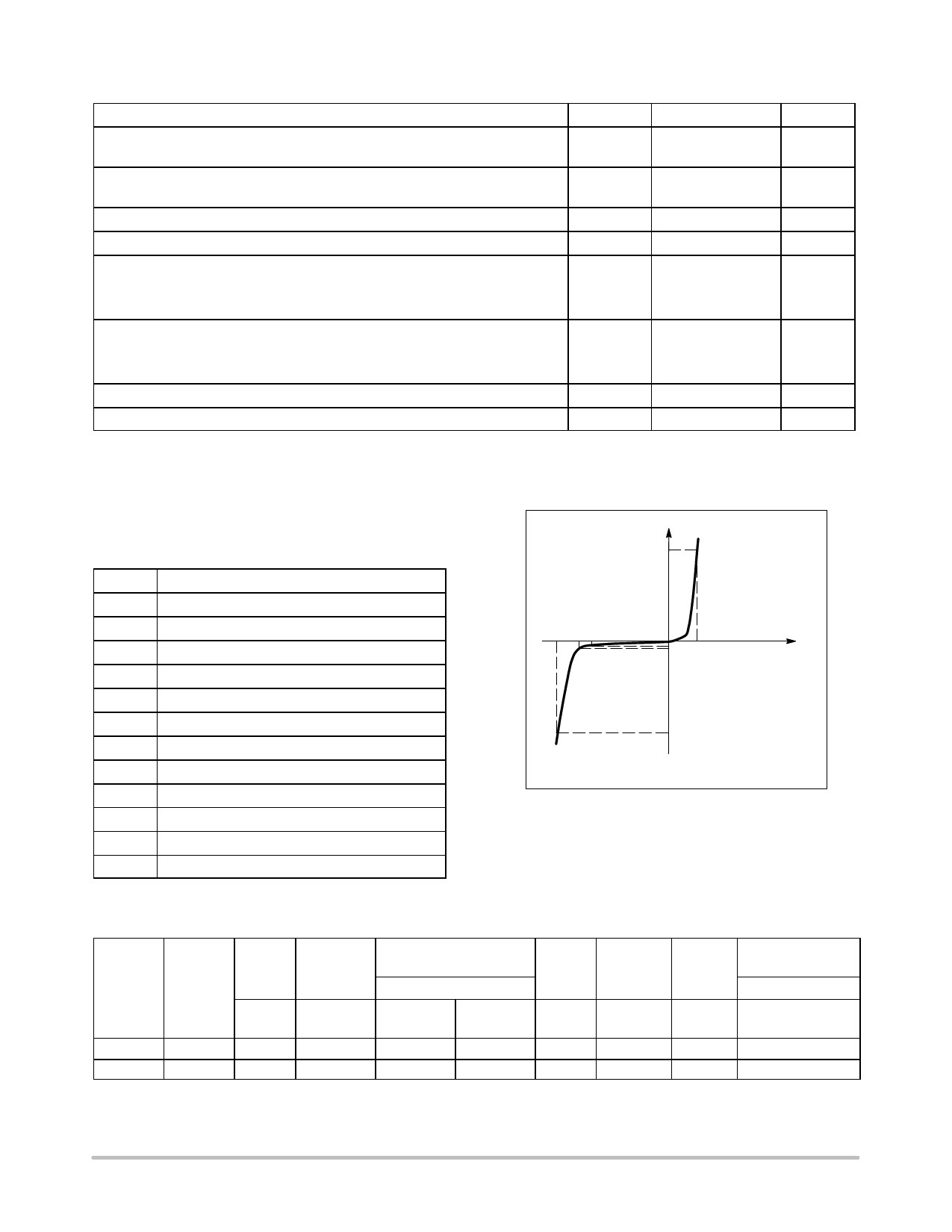
I
IF
VC VBR VRWM
IIRT VF
IPP
Uni−Directional
Unit
Watts
kV
A
A
°mW°
mW/°C
°C/W
°mW
mW/°C
°C/W
°C
°C
V
ELECTRICAL CHARACTERISTICS
Device
Device
Marking
VRWM
(Volts)
IR @ VRWM
(mA)
SM12T1
12M
12
1.0
4. 8 × 20 ms pulse waveform per Figure 3
VBR, Breakdown Voltage
(Volts)
Min
Max
13.3
15.75
VC @
IPP = 1 Amp
(Volts)
19
Max IPP
(Note 4)
(Amps)
12
Typical Capacitance
(pF)
Pin 1 to 3 @ 0 Volts
95
www.onsemi.com
2
Share Link: 