M62254FP Просмотр технического описания (PDF) - Renesas Electronics
Номер в каталоге
Компоненты Описание
производитель
M62254FP Datasheet PDF : 12 Pages
| |||
M62254FP
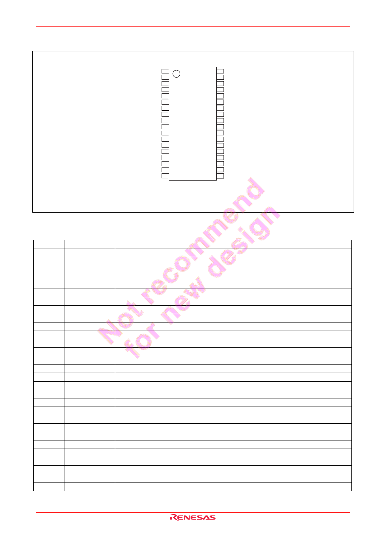
Pin Arrangement
OPIN1+ 1
OPIN1− 2
LED1 3
LED2 4
LED3 5
P.GND 6
MSW1 7
MSW2 8
SSW 9
CD 10
REF 11
IN1 12
IN2 13
IN3 14
IN4 15
ISENSE 16
DOUT 17
RESET 18
M62254FP
(Top view)
36 OPOUT1
35 OPOUT2
34 OPIN2+
33 OPIN2−
32 P.C
31 GND
30 Iadj
29 IDET
28 VDET
27 TC
26 WD
25 Ctd
24 CS
23 CK
22 DI
21 VB
20 VCC
19 VDD
Outline: PRSP0036GA-A (36P2R-A)
Pin Description
Pin No.
24
23
Pin Name
CS
CK
22
DI
17
11
12 to 15
16
10
9
7, 8
3 to 5
19
21
20
29
30
28
32
2, 33
1, 34
36, 35
31
6
18
27
26
25
DOUT
REF
IN1 to IN4
ISENSE
CD
SSW
MSW1, MSW2
LED1 to LED3
VDD
VB
Vcc
IDET
Iadj
VDET
P.C
OPIN1–, OPIN2–
OPIN1+, OPIN2+
OPOUT1, OPOUT2
GND
P.GND
RESET
TC
WD
Ctd
Function
The serial data input pin which used to receives 8-bit wide serial data.
The shift clock input pin which takes the input signal of DI pin to 8-bit shift register by the
rising edge of the clock signal.
When CS pin is "Low", this pin can receive the data into the 8-bit shift register. The each
bit will be latched at rising edge of the clock signal.
The output pin of the amplified A/D input.
The reference voltage output pin of the A/D converter.
The A/D converter input pin.
The current sense input pin.
The input pin for the current detection to feedback of sub-switch driver.
The sub-switch driver output pin.
The main switch driver output pin. (Open collector)
The LED driver output pin. (Open collector)
The stabilized +5 V output pin.
The pre-drive pin which used to connect the external PNP Tr.
The power supply pin.
The current detection input pin.
The input pin for current detection adjustment.
The voltage detection input pin.
The feedback pin for voltage and current control.
The inverted input pin of OP-amp.
The non-inverted input pin of OP-amp.
The OP-amp. output pin. (Open collector output)
The ground pin.
The ground pin of power unit. (Main switch driver and LED driver)
The output pin of Reset and WDT. (Pulled up to VDD)
The pin used to connect capacitor to determine the time constant of WDT.
The input pin of the WDT.
The pin used to connect capacitor to determine delay time the output after the Reset.
REJ03F0244-0200 Rev.2.00 Jun 16, 2008
Page 2 of 11
Share Link: 