L6660 Просмотр технического описания (PDF) - STMicroelectronics
Номер в каталоге
Компоненты Описание
производитель
L6660 Datasheet PDF : 9 Pages
| |||
L6660
ELECTRICAL CHARACTERISTICS (continued)
Symbol
Vout0
VrefOUT
Ivref
Vref, cap
Vshifted
Shifter Gain
Parameter
OpAmp Output Voltage with 0V
Input Voltage
Reference Voltage PIN13
Reference Voltage Output Current
Filter capacitor at PIN13
Voltage shift value
(VPIN11 - VPIN10)
Analog Voltage Shifter DC
Voltage Gain
∆V10
∆V11
Test Condition
External feedback programmed
for DC gain value <30V/V
1.0V ≤ Vin0-5 ≤ 3.5V
VPIN11 = VREFIN → V’10
VPIN11 = VREFIN + 0.1V → V"10
G
=
V’’10 − V’10
0.1
BWVshift
VrefIN
Isleep
EAoff
IEA
HVP%
Vlogic0
Vlogic1
Ztime
Top
Shifter circuitry Band Width
External reference voltage
(PIN14)
Total current in Sleep Mode
DC-DC converter Error
Amplifier Input voltage Offset
(VPIN14-VPIN21)
Error amplifier Current
Capability
Total HVP precision
Voltage level for 0 logic at
digital input pin (Pin 1-4-7-15)
Voltage level for 1 logic at
digital input pin (Pin 1-4-7-15)
Decay period for ∆V = |19V|
Operative period from Not
Selected phase to Selected
phase for each driver
3dB amplitude drop
PIN7 at 0 logic
VrefIN = 2.25V
Vref = 2.25V±0%
Vref (Pin14) = 2.25V See Fig. 3
0°C < Tcase < 80°C
Min.
-1
2.4
-1
10
VrefIN
-2%
0.975
2.0
-12
-4
1.6
140
Typ.
2.5
VrefIN
1.00
2
±100
Max.
+1
2.6
+1
100
VrefIN
+2%
1.025
2.6
800
+12
+4
0.9
340
4
Unit
V
V
mA
nF
V
MHz
V
µA
mV
µA
%
V
V
µs
µs
Note 1: Selectable by external resistors.
Note 2: Set by external Coil and Capacitor from 80 to 550KHz.
Note 3: Take into account the total power dissipation.
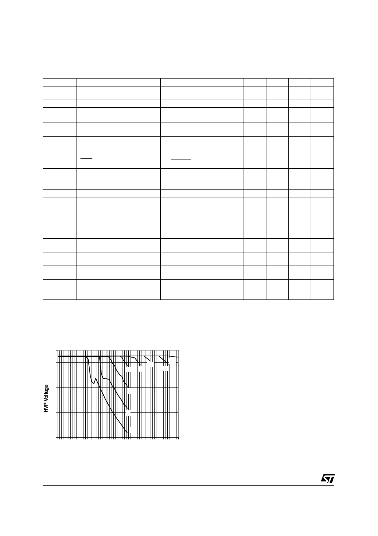
Figure 1. Load Regulation
36
34
12V
10V
8V 9V
11V
32
30
7V
28
26
6V
24
5V
22
1 5 9 13 17 21 25 29 33 37 41 45 49 53 57 61 65
Load DC Current (mA)
OPERATIONAL AMPLIFIERS DESCRIPTION
Each driver has two output stages scaled in cur-
rent by a factor K = 10.
In voltage mode configuration the two outputs are
shorted.
In charge mode configuration OUT1 drives a ca-
pacitor Cint and is closed in feedback, while
OUTK drives the piezo, mirroring the current sup-
plied to Cint, with a current multiplied by a K fac-
tor (see Fig.2).
The supply voltage can be internally generated
by the DC-DC converter, or external, maintaining
the DC-DC converter in sleep mode (PIN3
shorted to ground), in this case the supply volt-
age can be 0 to V5/12+4 minimum value up to
70V in single supply or V5/12+4 to 35V symmetri-
cal to ground.
The drivers have 130dB DC gain and the Band-
width is 500KHz. Stability is guaranteed with a
minimum gain of 20dB, for a capacitive load in
the range 0.4nF up to 24nF.
4/9
Share Link: 