EN5312QI Просмотр технического описания (PDF) - Enpirion, Inc.
Номер в каталоге
Компоненты Описание
производитель
EN5312QI Datasheet PDF : 16 Pages
| |||
EN5312QI
1A Synchronous Buck Regulator
With Integrated Inductor
Revised March 2007
RoHS Compliant
Featuring Integrated Inductor Technology
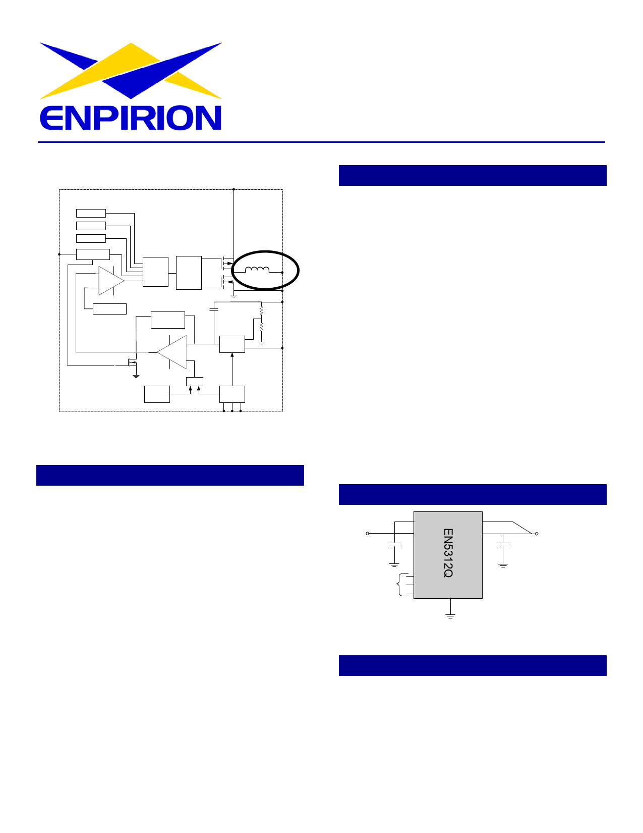
VIN
ENABLE
UVLO
Thermal Limit
Current Limit
Soft Start
(-)
PWM
Comp
(+)
Sawtooth
Generator
Logic
P-Drive
N-Drive
Compensation
Network
(-)
Error
Amp
(+)
VREF
DAC
Switch
VOUT
GND
VSENSE
VFB
Voltage
Select
Package Boundry
VS0 VS1 VS2
Product Highlights
• Integrated Planar Inductor
• Designed for low noise/low EMI
• Very small solution foot print*
• Only two low cost MLCC caps required
• RoHS compliant; MSL 3 260°C reflow
• 5mm x 4mm x1.1mm QFN package
• Wide 2.4V to 5.5V input range
• 1000mA continuous output current
• Less than 1 µA standby current.
• High efficiency, up to 95%
• Excellent transient performance
• Very low ripple voltage; 5mVp-p Typical
• 3 Pin VID Output Voltage select
• External divider: 0.6V to VIN-Vdropout
• 4 MHz switching frequency
• 100% duty cycle capable
• Short circuit and over current protection
• UVLO and thermal protection
Product Overview
The Ultra-Low-Profile EN5312QI is targeted to
applications where board area and profile are
critical. EN5312QI is a complete power
conversion solution requiring only two low cost
ceramic MLCC caps. Inductor, MOSFETS,
PWM, and compensation are integrated into a
tiny 5mm x 4mm x 1.1mm QFN package. The
EN5312QI is engineered to simplify design and
to minimize layout constraints. 4 MHz
switching frequency and internal type III
compensation provides superior transient
response. With a 1.1 mm profile, the
EN5312QI is ideal for space and height
constrained applications.
A 3-pin VID output voltage selector provides
seven pre-programmed output voltages along
with an option for external resistor divider.
Output voltage can be programmed on-the-fly
to provide fast, dynamic voltage scaling.
Typical Application Circuit
VIN
4.7µF
Voltage
Select
ENABLE
Vin
VSense
Vout
VFB
VS0
VS1
VS2
GND
VOUT
10µF
Figure 1. Typical application circuit.
Applications
• LDO replacement for improved thermals
• FPGA, DSP, ASIC, IO & Peripherals
• Area constrained applications
• Set top box/home gateway
• Smart phones and PDAs
• VoIP and Video phones
• Personal Media Players
*Optimized PCB Layout file downloadable from the Enpirion Website to assure first pass design success.
Share Link: 