FXL2T245 Просмотр технического описания (PDF) - ON Semiconductor
Номер в каталоге
Компоненты Описание
производитель
FXL2T245 Datasheet PDF : 13 Pages
| |||
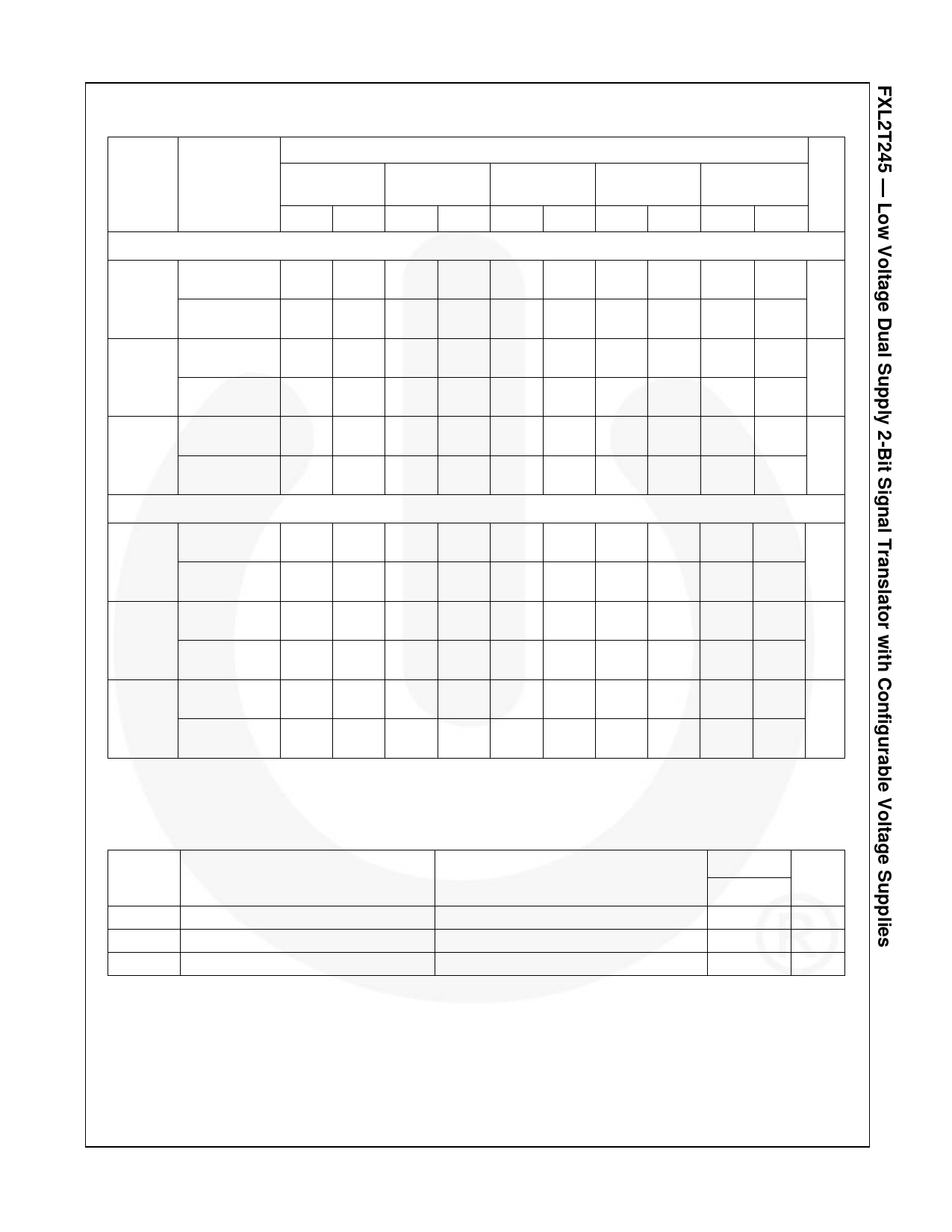
AC Electrical Characteristics
Symbol Parameter
VCCB=3.0 V
to 3.6 V
Min. Max.
VCCA=1.4 V to 1.6 V
Propagation
Delay A to B
0.5 4.3
tPLH, tPHL Propagation
Delay B to A
0.6
6.8
Output Enable
/OE to B
1.1
7.5
tPZH, tPZL Output Enable
/OE to A
1.0
7.5
Output Disable
/OE to B
0.4
6.1
tPHZ, tPLZ Output Disable
/OE to A
1.0
6.0
VCCA=1.1 V to 1.3 V
Propagation
Delay A to B
0.8
tPLH, tPHL Propagation
Delay B to A
1.4
Output Enable
/OE to B
1.0
tPZH, tPZL Output Enable
/OE to A
2.0
Output Disable
/OE to B
1.0
tPHZ, tPLZ Output Disable
/OE to A
2.0
13.0
22.0
12.0
22.0
15.0
15.0
TA= -40 to +85°C
VCCB=2.3 V
to 2.7 V
VCCB=1.65 V
to 1.95 V
VCCB=1.4 V
to 1.6 V
Min. Max. Min. Max. Min. Max.
0.5 4.8 1.0 6.0 1.0 7.3
0.8 6.9 0.9 7.1 1.0 7.3
1.1 7.6 1.3 7.7 1.4 7.9
1.0 7.5 1.0 7.5 1.0 7.5
0.4 6.2 0.9 6.2 1.5 7.5
1.0 6.0 1.0 6.0 1.0 6.0
1.0 7.0 1.2 8.0 1.3 9.5
1.4 22.0 1.5 22.0 1.5 22.0
1.0 9.0 2.0 10.0 2.0 11.0
2.0 22.0 2.0 22.0 2.0 22.0
0.7 7.0 1.0 8.0 2.0 10.0
2.0 12.0 2.0 12.0 2.0 12.0
VCCB=1.1 V
to 1.3V
Unit
Min. Max.
1.5 22.0
ns
1.3 9.5
2.0 20.0
ns
1.0 7.5
2.0 18.0
ns
1.0 6.0
2.0 24.0
ns
2.0 24.0
2.0 24.0
ns
2.0 22.0
2.0 20.0
ns
2.0 12.0
Capacitance
Symbol
Parameter
Conditions
TA=+25°C
Typical
CIN Input Capacitance (Pins O/E, TR)
VCCA=VCCB=3.3 V, VI=0V or VCCA/B
4
CI/O Input / Output Capacitance An, Bn Ports VCCA=VCCB=3.3 V, VI=0V or VCCA/B
5
CPD Power Dissipation Capacitance
VCCA=VCCB=3.3 V, VI=0V or VCC, f=10 MHz
20
Unit
pF
pF
pF
© 2005 Fairchild Semiconductor Corporation
FXL2T245 • Rev. 1.0.2
8
www.fairchildsemi.com
Share Link: 