FXL2T245 Просмотр технического описания (PDF) - ON Semiconductor
Номер в каталоге
Компоненты Описание
производитель
FXL2T245 Datasheet PDF : 13 Pages
| |||
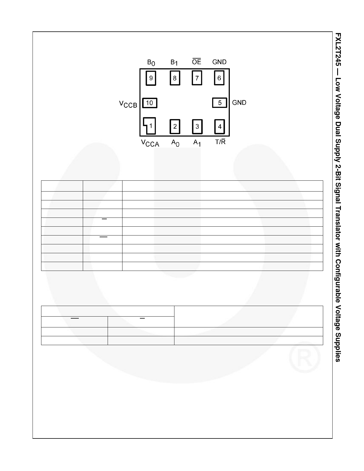
Pin Configuration
Figure 1. Pin Assignments
Pin Descriptions
Pin#
1
2
3
4
5, 6
7
8
9
10
Pin Name
VCCA
A0
A1
T/R
GND
O/E
B1
B0
VCCB
Description
Side A Power Supply
Side A Inputs or 3-State Outputs
Side A Inputs or 3-State Outputs
Transmit/Receive Input
Ground
Output Enable Input
Side B Inputs or 3- State Outputs
Side B Inputs or 3-State Outputs
Side B Power Supply
Truth Table
Inputs
OE
LOW
LOW
Notes:
1. LOW = low voltage level.
2. HIGH = high voltage level.
T/R
LOW
HIGH
Outputs
Bus B Data to Bus A
Bus A Data to Bus B
© 2005 Fairchild Semiconductor Corporation
FXL2T245 • Rev. 1.0.2
2
www.fairchildsemi.com
Share Link: 