SPX2920T-5.0 Просмотр технического описания (PDF) - Signal Processing Technologies
Номер в каталоге
Компоненты Описание
производитель
SPX2920T-5.0 Datasheet PDF : 10 Pages
| |||
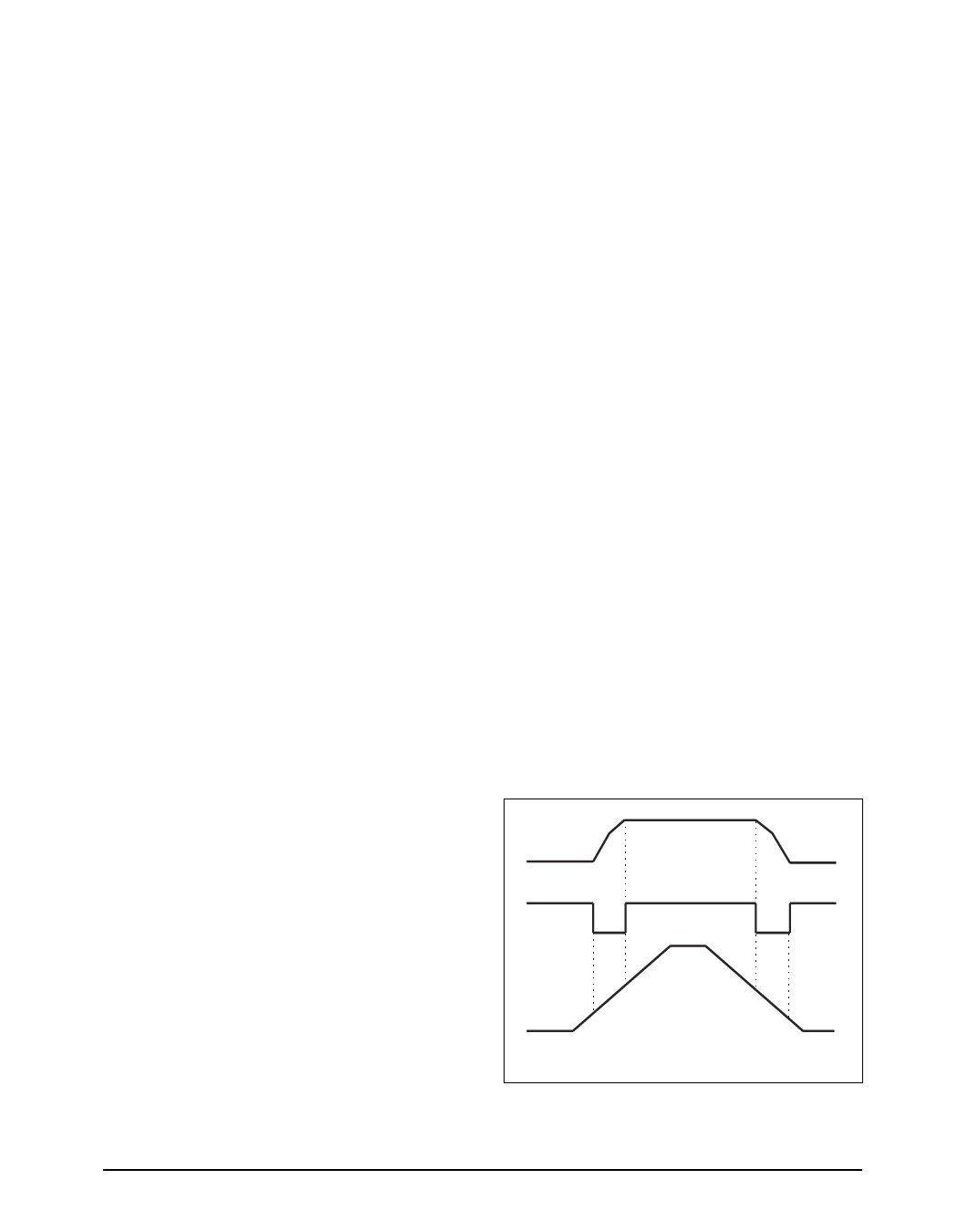
Error Detection Comparator Output
The Comparator produces a logic low output
whenever the SPX2920 output falls out of regu-
lation by more than around 5%. This is around
60mV offset divided by the 1.235 reference
voltage. This trip level remains 5% below
normal regardless of the programmed output
voltage of the regulator. Figure 1 shows the
timing diagram depicting the ERROR signal
and the regulator output voltage as the SPX2920
input is ramped up and down. The ERROR
signal becomes low at around 1.3V input, and
goes high around 5V input (input voltage at
which VOUT = 4.75). Since the SPX2920’s
dropout voltage is load dependent, the input
voltage trip point (around 5V) will vary with the
load current. The output voltage trip point
(approx. 4.75V) does not vary with load.
The error comparator has an open-collector out-
put, which requires an external pull-up resistor.
Depending on the system requirements the re-
sistor may be returned to 5V output or other
supply voltage. In determining the value of this
resistor, note that the output is rated to sink
400µA; this value adds to battery drain in a low
battery condition. Suggested values range from
100K to 1MΩ. If the output is unused this
resistor is not required.
Programming the Output Voltage of
SPX2920
The SPX2920 may be pin-strapped for 5V or
3.3V using its internal voltage divider by tying
Pin 1 (output) to Pin 2 (sense) and Pin 7 (feed-
back) to Pin 6 (5V/3.3V Tap).
Also, it may be programmed for any output
voltage between its 1.235V reference and its
20V maximum rating. As seen on the front
page, an external pair of resistors is required.
Refer to the below equation for the program-
ming of the output voltage::
VOUT = VREF x ( 1 + R1/ R2 )+ IFBR1
The VREF is 1.235 and IFB is the feedback bias
current, nominally -20nA. The minimum rec-
ommended load current of 1µA forces an upper
limit of 1.2MΩ on value of R2. If no load is
presented the I produces an error of typically
FB
2% in VOUT, which may be eliminated at room
temperature by trimming R1. To improve the
accuracy choose the value of R2 = 100k; this
reduces the error by 0.17% and increases the
resistor program current by 12µA. Since the
SPX2920 typically draws 60 µA at no load with
Pin 2 open-circuited this is a small price to pay.
Reducing Output Noise
It may be an advantage to reduce the AC noise
present at the output. One way is to reduce the
regulator bandwidth by increasing the size of
the output capacitor. This is the only way that
noise can be reduced on the 3 lead SPX2920 but
is relatively inefficient, as increasing the ca-
pacitor from 1µF to 220µF only decreases the
noise from 430µV to 160µV Vrms for a 100kHz
bandwidth at 5V output.
Noise could also be reduced fourfold by a by-
pass capacitor across R1, since it reduces the
high frequency gain from 4 to unity. Pick
C
BYPASS
≅1
/
2πR1
x
200
Hz
or choose 0.01µF. When doing this, the output
capacitor must be increased to 3.3µF to main-
tain stability. These changes reduce the output
noise from 430µV to 100µV Vrms for a 100kHz
bandwidth at 5V output. With the bypass ca-
pacitor added, noise no longer scales with out-
put voltage so that improvements are more dra-
matic at higher output voltages.
4.75V
OUTPUT
VOLTAGE
_______
ERROR*
INPUT
VOLTAGE
+5.0V
+1.3V
* See Application Info.
+
+
Figure 1. ERROR Output Timing
Rev: A Date: 03/30/04
SPX2920 400mA Low Drop Out Voltage Regulator with Shutdown
5
©Copyright 2004 Sipex Corporation
Share Link: 