MSK5150 Просмотр технического описания (PDF) - Anaren Microwave
Номер в каталоге
Компоненты Описание
производитель
MSK5150 Datasheet PDF : 7 Pages
| |||
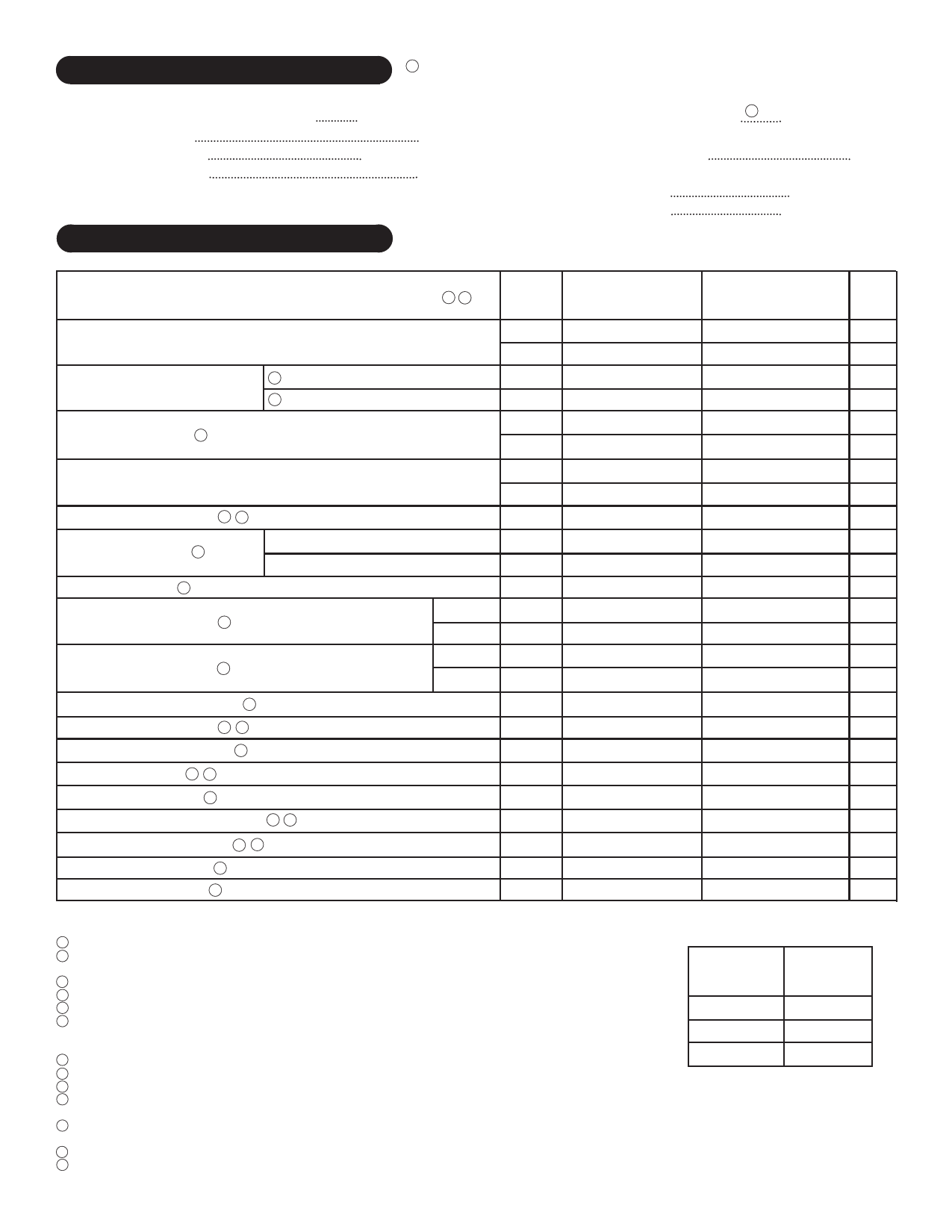
ABSOLUTE MAXIMUM RATINGS 12
VINP Input Voltage (100mS 1%D.C.)
VIN Input Voltage
VEN Enable Voltage
IOUT Output Current
-20V to +60V
26V
-0.3V to 26V
5.0A
ELECTRICAL SPECIFICATIONS
TST Storage Temperature Range 13
TLD Lead Temperature
(10 Seconds Soldering)
TJ Operating Temperature
MSK5150 Series
MSK5150B Series
-65°C to +150°C
300°C
-40°C to +85°C
-55°C to +125°C
Parameter
Test Conditions 1 3
Group A MSK5150B SERIES
MSK5150 SERIES
Subgroup Min. Typ. Max. Min. Typ.
Max. Units
Output Voltage Tolerance
IOUT=10mA; VIN=VOUT+1V
1
-
±0.5 ±1.0 -
±0.5
±1.0 %
2,3
-
±1.0 ±2.0 -
-
-
%
Dropout Voltage
2
∆VOUT=-1%; IOUT=250m A
2
∆VOUT=-1%; IOUT=5A
1
-
125 250 -
125
275 mV
1
-
370 600 -
370
625 mV
Load Regulation 10
VIN=VOUT+1V
10mA ≤ IOUT ≤ 4.5A
1
-
±0.2 ±1.0 -
±0.2
±1.2 %
2,3
-
±0.3 ±2.0 -
±0.3
-
%
Line Regulation
(VOUT +1V) ≤ VIN≤ 26V
IOUT=10mA
1
-
±0.05 ±0.5 -
±0.05 ±0.6 %
2,3
-
±0.5 ±1.0 -
±0.5
-
%
Output Current Limit 2 11
VOUT=0V; VIN=VOUT+1V
-
-
7.5
10 -
7.5
10
A
Ground Current 2
VIN=VOUT+1V; IOUT=2.5A
VIN=VOUT+1V; IOUT=5A
-
-
15
50 -
15
55 mA
-
-
70
-
-
70
-
mA
Output Noise 2
CL=20µF; 10Hz ≤ f ≤ 100KHz
-
-
400
-
-
400
-
µV
Enable Input Voltage 2
HIGH/ON
1
LOW/OFF
1
2.4
1.2
- 2.4
1.2
-
1.2
0.8 -
1.2
-
V
0.8
V
Enable Input Current 2
HIGH/ON
1
LOW/OFF
1
-
100 600 -
100
600 µA
-
-
2
-
-
2
µA
Shutdown Output Current 2
VENABLE ≤ 0.8V
-
-
10
500 -
10
500 µA
Flag Output Leakage 2 9
VOH=26V
-
-
0.01
2
-
0.01
2
µA
Flag Output On Voltage 9
IOL ≤ 250µA; VIN=VOUT-2V
1
-
0.2
0.4 -
0.2
0.4
V
Flag Threshold 2 9
VIN=VOUT-7%
-
-
75
-
-
75
-
mV
Reference Voltage 8
Normal Operation
1
1.22 1.24 1.26 1.22 1.24
1.26 V
Reference Voltage Temp Drift 2 8
Normal Operation
-
-
20
-
-
20
- ppm/°C
Adjust Pin Bias Current 2 8
Full Temp; VIN=VOUT+1V
-
-
40
120 -
40
150 nA
Thermal Resistance 2
Junction to Case @125°C
-
-
1.1
1.5 -
1.1
1.7 °C/W
Thermal Shutdown 2
TJ
-
-
135
-
-
135
-
°C
NOTES:
1 Output decoupled to ground using 28µF minimum capacitance unless otherwise specified.
2 This parameter is guaranteed by design but need not be tested.
Typical parameters are representative of actual device performance but are for reference only.
3 All output parameters are tested using a low duty cycle pulse to maintain TJ = TC.
4 Industrial grade devices shall be tested to subgroup 1 unless otherwise specified.
5 Military grade devices ('B' suffix) shall be 100% tested to subgroups 1,2 and 3.
6 Subgroup 1
TC=+25°C
Subgroup 2
TJ=+125°C
Subgroup 3
TA=-55°C
7 Please consult the factory if alternate output voltages are required.
8 Applies to MSK5150-00 adjustable version only.
9 Applies to fixed output devices only.
10 Due to current limit, maximum output current may not be available at all values of VIN-VOUT and temperatures. See typical
performance curves for clarification.
11 The output current limit function provides protection from transient overloads but it may exceed the maximum continuous rating.
Continuous operation in current limit may damage the device.
12 Continuous operation at or above absolute maximum ratings may adversely effect the device performance and/or life cycle.
13 Internal solder reflow temperature is 180°C, do not exceed.
PART
NUMBER
MSK5150-00
MSK5150-3.3
MSK5150-5.0
OUTPUT
VOLTAGE
Adjustable
+3.3V
+5.0V
2
8548-48 Rev. J 1/16
Share Link: 