LC75055PE-6158-H Просмотр технического описания (PDF) - ON Semiconductor
Номер в каталоге
Компоненты Описание
производитель
LC75055PE-6158-H Datasheet PDF : 26 Pages
| |||
LC75055PE
Specifications
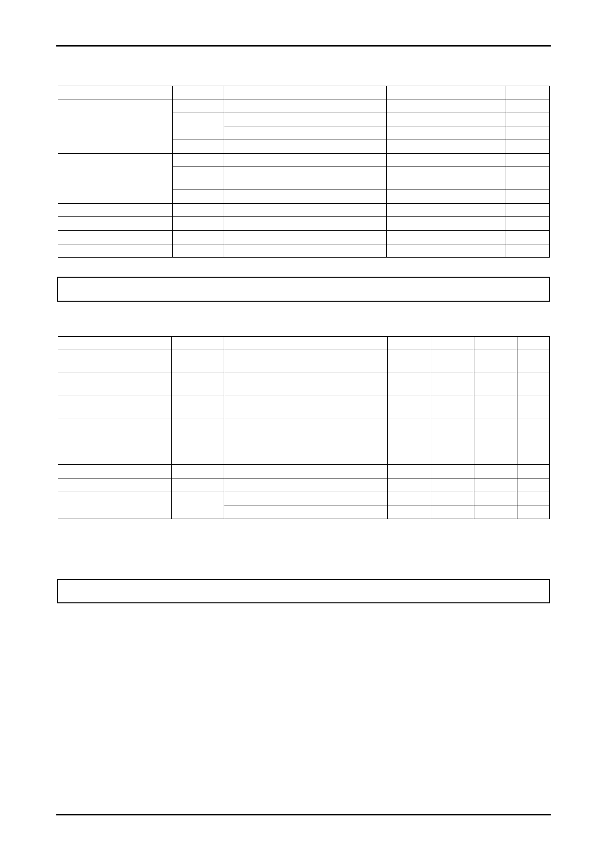
Absolute Maximum Ratings at Ta = 25C, DVSS_1 to 3 = COAVSS1 to 6 =AVB = XVSS = AVCOVSS = 0V
Parameter
Maximum supply voltage
Symbol
VDD max1
VDD max2
Applicable pins
CODEC power supply pin
Power supply pin for oscillation circuit
Digital 3.3V power supply pin
Ratings
Unit
-0.3 to +3.9
V
-0.3 to +3.9
V
-0.3 to +3.9
V
Maximum input voltage
Maximum output current
Allowable power dissipation
VDD max3
VIN1
VIN2
VIN3
IO
Pd max
Logic (DSP)
CODEC Analog input pin
Oscillation circuit input pin, TEST setting input
pin
Digital input pin
All output pin
Ta = 85C (Note 1)
-0.3 to +1.8
V
-0.3 to VDD max1 +0.3
V
-0.3 to VDD max2 +0.3
V
-0.3 to +6.0
V
6.0
mA
900
mW
Operating temperature
Topr
-40 to +85
C
Storage temperature
Tstg
-55 to +125
C
Note 1: For a chip mounted on a reference board. (board size: 105 75 1.6mm 4-layer)
Stresses exceeding those listed in the Maximum Ratings table may damage the device. If any of these limits are exceeded, device functionality should not be assumed,
damage may occur and reliability may be affected.
Allowable Operating Range at Ta = -40 to 85C, DVSS_1 to 3 = COAVSS1 to 6 =AVB = XVSS = AVCOVSS = 0V
Parameter
Symbol
Applicable pins
min
typ
max
Unit
Supply voltage
CODEC ANALOG
Supply voltage
XTAL, DSP_IO
Supply voltage
PLL
Supply voltage
Logic
Input high level voltage
Input high level voltage
Input low level voltage
Crystal oscillation frequency
(256fs)
AVDD
DVDD33
AVCOVDD
DVDD
VIH1
VIH2
VIL1
Fosc
CODEC power supply pin
Power supply pin for oscillation circuit
Digital 3.3V power supply pin
Power supply pin for PLL
Power supply pin for Logic
All digital input pin except for XIN
XIN
All digital input pin
XIN, XOUT (fs = 44.1kHz) *2
XIN, XOUT (fs = 48kHz) *2
3.14
3.3
3.47
V
3.14
3.3
3.47
V
3.14
3.3
3.47
V
1.43
1.5
1.58
V
2.0
5.5
*1
V
2.0
DVDD33
V
0
0.8
V
11.2896
MHz
12.288
MHz
*1) Only when power is supplied to all the power supplies, you can supply power to input pin up to 5.5V.
When the power is turned off, only supply the power up to 3.6V.
*2) Crystal for oscillator CI value: CI 150
The evaluation by the crystal supplier is recommended.
Functional operation above the stresses listed in the Recommended Operating Ranges is not implied. Extended exposure to stresses beyond the Recommended
Operating Ranges limits may affect device reliability.
No.A2168-2/26
Share Link: 