MW7IC2040N Просмотр технического описания (PDF) - NXP Semiconductors.
Номер в каталоге
Компоненты Описание
производитель
MW7IC2040N Datasheet PDF : 29 Pages
| |||
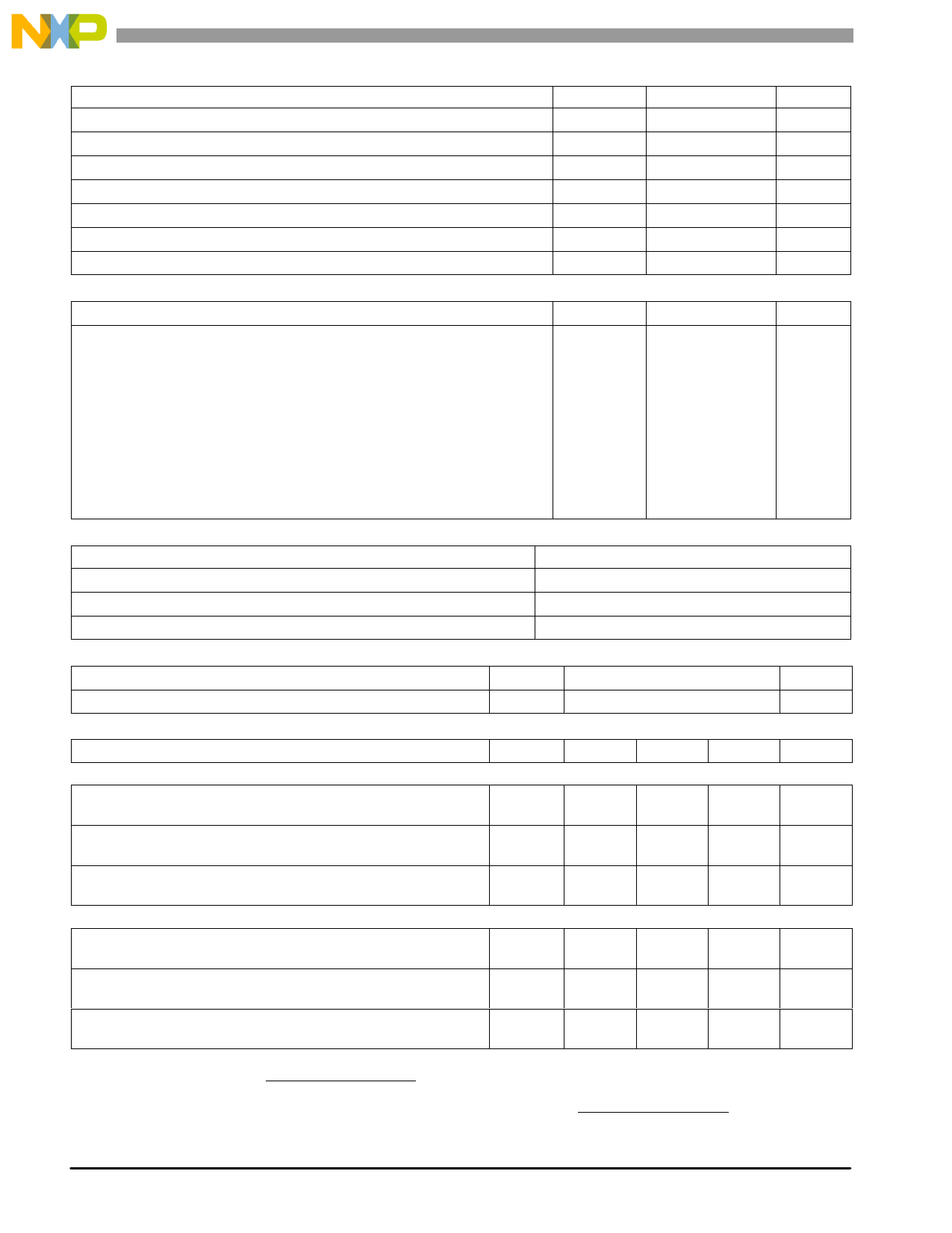
Table 1. Maximum Ratings
Rating
Drain - Source Voltage
Gate - Source Voltage
Operating Voltage
Storage Temperature Range
Case Operating Temperature
Operating Junction Temperature (1,2)
Input Power
Table 2. Thermal Characteristics
Characteristic
Thermal Resistance, Junction to Case
Symbol
VDSS
VGS
VDD
Tstg
TC
TJ
Pin
Symbol
RθJC
Value
- 0.5, +65
- 0.5, +10
32, +0
- 65 to +150
150
225
25
Value (2,3)
Unit
Vdc
Vdc
Vdc
°C
°C
°C
dBm
Unit
°C/W
W - CDMA
(Pout = 4 W Avg., Case Temperature = 73°C) Stage 1, 28 Vdc, IDQ1 = 130 mA
4.0
Stage 2, 28 Vdc, IDQ2 = 330 mA
1.5
GSM EDGE
(Pout = 16 W Avg., Case Temperature = 76°C) Stage 1, 28 Vdc, IDQ1 = 130 mA
4.1
Stage 2, 28 Vdc, IDQ2 = 330 mA
1.4
GSM
(Pout = 40 W Avg., Case Temperature = 79°C) Stage 1, 28 Vdc, IDQ1 = 130 mA
3.9
Stage 2, 28 Vdc, IDQ2 = 330 mA
1.3
Table 3. ESD Protection Characteristics
Test Methodology
Class
Human Body Model (per JESD22 - A114)
1B (Minimum)
Machine Model (per EIA/JESD22 - A115)
A (Minimum)
Charge Device Model (per JESD22 - C101)
III (Minimum)
Table 4. Moisture Sensitivity Level
Test Methodology
Rating
Package Peak Temperature
Unit
Per JESD22 - A113, IPC/JEDEC J - STD - 020
3
260
°C
Table 5. Electrical Characteristics (TC = 25°C unless otherwise noted)
Characteristic
Symbol
Min
Typ
Max
Unit
Stage 1 — Off Characteristics
Zero Gate Voltage Drain Leakage Current
(VDS = 65 Vdc, VGS = 0 Vdc)
Zero Gate Voltage Drain Leakage Current
(VDS = 28 Vdc, VGS = 0 Vdc)
Gate - Source Leakage Current
(VGS = 1.5 Vdc, VDS = 0 Vdc)
IDSS
—
—
10
μAdc
IDSS
—
—
1
μAdc
IGSS
—
—
1
μAdc
Stage 1 — On Characteristics
Gate Threshold Voltage
(VDS = 10 Vdc, ID = 25 μAdc)
VGS(th)
1.2
2
2.7
Vdc
Gate Quiescent Voltage
(VDS = 28 Vdc, IDQ1 = 130 mAdc)
VGS(Q)
—
2.7
—
Vdc
Fixture Gate Quiescent Voltage
(VDD = 28 Vdc, IDQ1 = 130 mAdc, Measured in Functional Test)
VGG(Q)
13
14.5
16
Vdc
1. Continuous use at maximum temperature will affect MTTF.
2. MTTF calculator available at http://www.freescale.com/rf. Select Software & Tools/Development Tools/Calculators to access MTTF
calculators by product.
3. Refer to AN1955, Thermal Measurement Methodology of RF Power Amplifiers. Go to http://www.freescale.com/rf.
Select Documentation/Application Notes - AN1955.
(continued)
MW7IC2040NR1 MW7IC2040GNR1 MW7IC2040NBR1
2
RF Device Data
Freescale Semiconductor
Share Link: 