MCF5270CAB100 Просмотр технического описания (PDF) - Freescale Semiconductor
Номер в каталоге
Компоненты Описание
производитель
MCF5270CAB100 Datasheet PDF : 42 Pages
| |||
Design Recommendations
5.2.1 Supply Voltage Sequencing and Separation Cautions
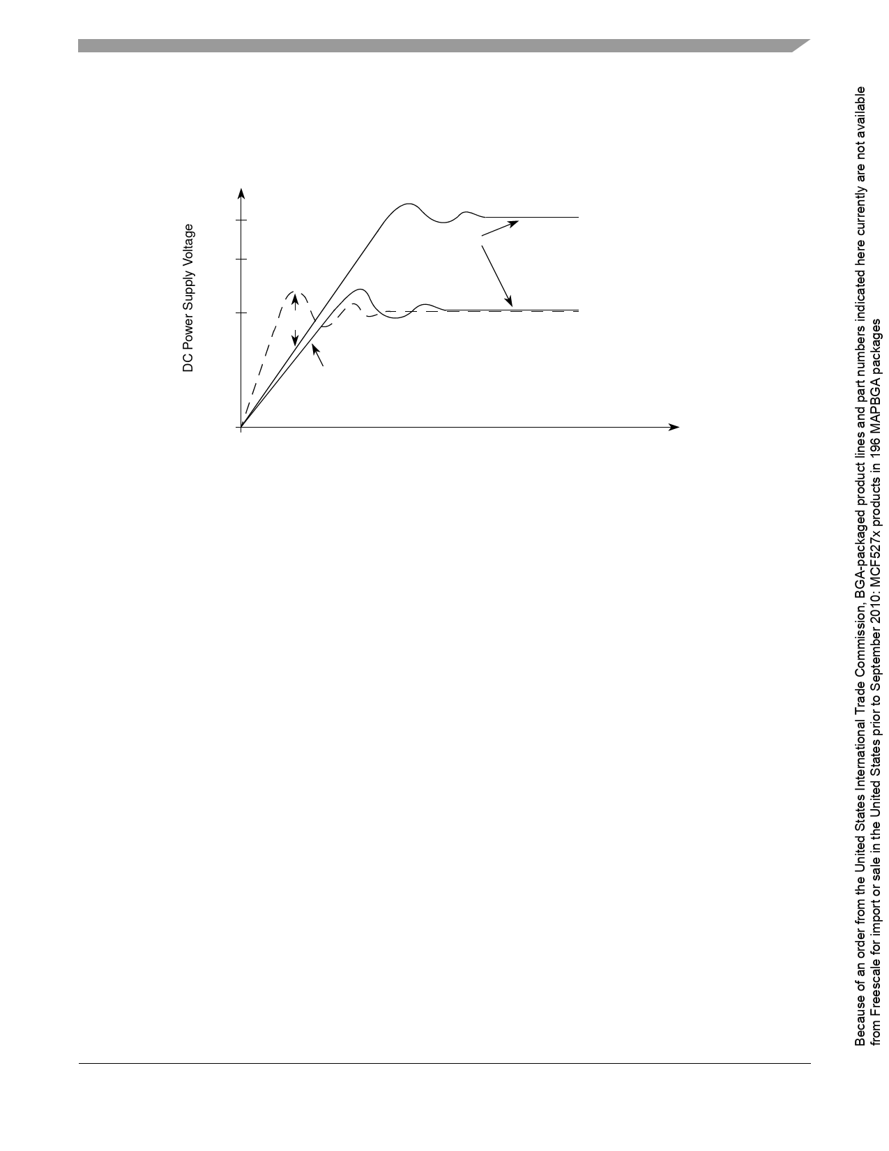
Figure 2 shows situations in sequencing the I/O VDD (OVDD), PLL VDD (VDDPLL), and Core VDD (VDD).
OVDD is specified relative to VDD.
3.3V
2.5V
1.5V
1
Supplies Stable
OVDD, VDDPLL
VDD
2
0
Notes:
Time
1. VDD should not exceed OVDD or VDDPLL by more than 0.4 V
at any time, including power-up.
2. Recommended that VDD should track OVDD/VDDPLL up to
0.9 V, then separate for completion of ramps.
3. Input voltage must not be greater than the supply voltage (OVDD,
VDD, or VDDPLL) by more than 0.5 V at any time, including during power-up.
4. Use 1 ms or slower rise time for all supplies.
Figure 2. Supply Voltage Sequencing and Separation Cautions
5.2.1.1 Power Up Sequence
If OVDD is powered up with VDD at 0 V, then the sense circuits in the I/O pads cause all pad output drivers
connected to the OVDD to be in a high impedance state. There is no limit on how long after OVDD powers
up before VDD must power up. VDD should not lead the OVDD or VDDPLL by more than 0.4 V during
power ramp-up, or there will be high current in the internal ESD protection diodes. The rise times on the
power supplies should be slower than 1 μs to avoid turning on the internal ESD protection clamp diodes.
The recommended power up sequence is as follows:
1. Use 1 ms or slower rise time for all supplies.
2. VDD and OVDD/VDDPLL should track up to 0.9 V, then separate for the completion of ramps with
OVDD going to the higher external voltages. One way to accomplish this is to use a low drop-out
voltage regulator.
5.2.1.2 Power Down Sequence
If VDD is powered down first, then sense circuits in the I/O pads cause all output drivers to be in a high
impedance state. There is no limit on how long after VDD powers down before OVDD/VDDPLL must power
down. VDD should not lag OVDD or VDDPLL going low by more than 0.4 V during power down or there
MCF5271 Integrated Microprocessor Hardware Specification, Rev. 4
Freescale Semiconductor
9
Share Link: 