ATC100B0R1BT500XT Просмотр технического описания (PDF) - NXP Semiconductors.
Номер в каталоге
Компоненты Описание
производитель
ATC100B0R1BT500XT Datasheet PDF : 28 Pages
| |||
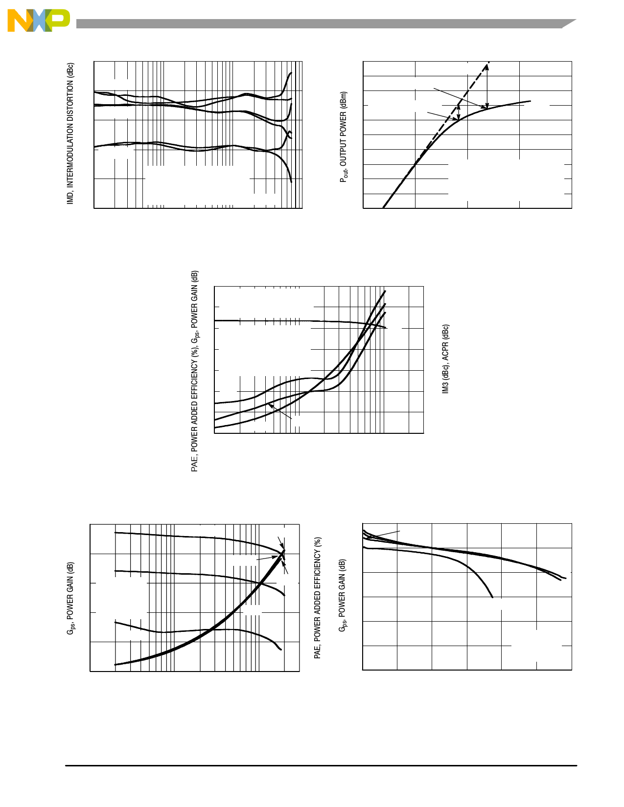
−30
−40 3rd Order
5th Order
−50
TYPICAL CHARACTERISTICS — 1930 - 1990 MHz
48
Ideal
P3dB = 44.8 dBm (30 W)
46
P1dB = 44 dBm (25 W)
44
Actual
−60 7th Order
−70
−80
0.1
VDD = 26 Vdc, Pout = 75 W (PEP)
IDQ1 = 100 mA, IDQ2 = 170 mA
Two−Tone Measurements
(f1 + f2)/2 = Center Frequency of 1960 MHz
1
10
100
TWO−TONE SPACING (MHz)
Figure 9. Intermodulation Distortion Products
versus Tone Spacing
42
VDD = 26 Vdc
40
IDQ1 = 100 mA, IDQ2 = 170 mA
Pulsed CW, 8 μsec(on), 1 msec(off)
f = 1960 MHz
38
10
15
20
25
30
Pin, INPUT POWER (dBm)
Figure 10. Pulsed CW Output Power versus
Input Power
35
VDD = 26 Vdc
30 IDQ1 = 100 mA, IDQ2 = 170 mA
f1 = 1955 MHz, f2 = 1965 MHz
25 2−Carrier W−CDMA
10 MHz Carrier Spacing
20 3.84 MHz Channel Bandwidth
PAR = 8.5 dB @ 0.01%
15 Probability (CCDF)
−25
−30
Gps
−35
−40
−45
10 IM3
−50
5
ACPR
0
PAE
0.1
1
−55
−60
10
30
Pout, OUTPUT POWER (WATTS) AVG.
Figure 11. 2 - Carrier W - CDMA ACPR, IM3, Power
Gain and Power Added Efficiency
versus Output Power
32
30
28 VDD = 26 Vdc
IDQ1 = 100 mA
IDQ2 = 170 mA
26 f = 1960 MHz
24
85_C
TC = −30_C
25_C
50
25_C
40
−30_C
PAE
85_C 30
Gps
20
10
22
0
0.1
1
10
30
Pout, OUTPUT POWER (WATTS) CW
Figure 12. Power Gain and Power Added
Efficiency versus CW Output Power
30
26 V
28
26
30 V
28 V
24
VDD = 20 V
22
IDQ1 = 100 mA
20
IDQ2 = 170 mA
f = 1840 MHz
18
0
5
10
15
20
25
30
Pout, OUTPUT POWER (WATTS) CW
Figure 13. Power Gain versus Output Power
RF Device Data
Freescale Semiconductor
MW6IC2015NBR1 MW6IC2015GNBR1
7
Share Link: 